Designing For Fab: A Heads-Up Before Designing PCBs For Professional Assembly

Designing pcbs for assembly is easy, right? We just squirt all the footprints onto a board layout, connect all the traces, send out the gerbers and position files, and we’re done–right?

Whoa, hold the phone, there, young rogue! Just like we can hack together some working source code with variables named after our best friends, we can also design our PCBs in ways that make it fairly difficult to assemble.

However, by following the agreed-upon design specs, we’ll put ourselves on track for success with automated assembly. If we want another party to put components on our boards, we need to clearly communicate the needed steps to get there. The best way to do so is by following the standards.

Proper Footprint Orientation

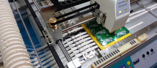
Now, for a momImage Credit: https://encrypted-tbn2.gstatic.com/images?q=tbn:ANd9GcQBEztpnSxpN_IRjq3y8GbetrMHKuoSu_s6myiFOHilL2FlQKyLrgent, let’s imagine ourselves as the tip of a vacuum pickup tool on a pick-and-place machine. These tools are designed to pick up components on the reel from their centroid and plunk them on their corresponding land pattern. Seems pretty straightforward, right? It is, provided that we design our footprints knowing that they’ll one day come face-to-face with the pick-and-place machine.

To get from the reel to the board, we, the designers, need two bits of information from out part’s datasheet: the part centroid and the reel orientation.

The part centroid is an X-Y location that calls out the center-of-mass of the part. It basically tells the machine: “pick me up from here!” As designers, it’s our responsibility to design all of our footprints such that the footprint origin is set at the part’s centroid. If we forget to do so, the pick-and-place will try to suck up our parts from a location that may not stick very well to the package, such as: the corner.

Continue reading “Designing For Fab: A Heads-Up Before Designing PCBs For Professional Assembly”

Bad Thermal Design And Burning Down The House

Control boards for 3D printers are a dime a dozen on the usual online marketplaces, and you usually get what you pay for. These boards can burn down your house thanks to a few terrible design choices. [Scott Rider] aka [Crow] took a look at the popular Melzi board, and what he found was horrifying. These boards overheat right at the connector for the heated bed, but the good news is these problems are easily fixed.

The Melzi board has a few problems with its PCB design. The first and most glaring issue is the use of thermals on the pads for the heated bed connector. In low-power applications, thermals — the method of not connecting the entire top or bottom layer to a hole or pad — are a great idea. It makes it easier to solder, because heat isn’t transmitted as easily to the entire copper layer. Unfortunately, this means heat isn’t transmitted as easily to the entire copper layer. In high-power applications, like a connection to a heated bed, these thermals can heat up enough to melt a plastic connector. Once that happens, it’s game over.

Other problems were found in the Melzi board, although you wouldn’t know it just by looking at the Eagle file of the PCB. [Scott]’s Chinesium Melzi board used 1-ounce copper, where 2-ounce copper would be more appropriate. The connector, too, should be rated above the design power loading.

[Scott] made a few tweaks to the board and also added a tiny DS1822Z temperature sensor to the high-current area of his version of a Melzi. Imagine that, 3D printer electronics with a temperature sensor. Slowly but surely, the state of 3D printer electronics is clawing its way to the present.

DIYing Huge BGA Packages

One day [Andy] was cruising around eBay and spotted something interesting. Forty Virtex-E FPGAs for two quid each. These are the big boys of the FPGA world, with 512 user IO pins, almost 200,000 logic gates, packed into a 676-ball BGA package. These are not chips designed for the hobbyist. These chips are not designed for boards with less than six layers. These chips aren’t even designed for boards with 6/6mil tolerances from the usual suspects in China. By any account, a 676-ball package is not like a big keep out sign for hobbyists. You don’t turn down a £2 class in advanced PCB design, though, leading to one of the most impressive ‘I just bought some crap on eBay’ projects we’ve seen.

halfbuiltThe project [Andy] had in mind for these chips was a generic dev board, which meant breaking out the IO pins and connecting some SRAM, SDRAM, and Flash memory. The first issue with this project is escape routing all the balls. Xilinx published a handy application note that recommends specific design parameters for the traces of copper under the chip. Unfortunately, this was a six-layer board, and the design rules in the application note were for 5/5mil traces. [Andy]’s board house can’t do six-layer boards, and their design rules are for 6/6mil traces. To solve this problem, [Andy] just didn’t route the inner balls, and hoped the 5mil traces would work out.

With 676 tiny little pads on a PCB, the clocks routed, power supply implemented, too many decoupling caps on the back, differential pairs, static RAM, a few LEDs placed just for fun, [Andy] had to solder this thing up. Since the FPGA was oddly one of the less expensive items on the BOM, he soldered that first, just to see if it would work. It did, which meant it was time to place the RAM, Flash, and dozens of decoupling caps. Everything went relatively smoothly – the only problem was the tiny 0402 decoupling caps on the back of the board. This was, by far, the hardest part of the board to solder. [Andy] only managed to get most of the decoupling caps on with a hot air gun. That was good enough to bring the board up, but he’ll have to figure some other way of soldering those caps for the other 30 or so boards.

Continue reading “DIYing Huge BGA Packages”

A Tale Of Two Browser PCB Tools

We live in a golden age of free Electronic Design Automation (EDA) tools. It wasn’t that long ago that an engineering workstation was an expensive piece of hardware running very expensive software that typically had annual fees. Now, you can go to your local electronics store and buy a PC that would shame that old workstation and download plenty of software to design schematics, simulate circuits, program devices, and lay out PCBs.

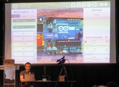
The only problem with a lot of this free software is it runs on Windows. I do sometimes run Windows, but I most often use Linux, so there is a certain attractiveness to a new breed of tools that run in the Web browser. In particular, I wanted to look briefly at two Web-based EDA tools: EasyEDA and MeowCAD. Both offer similar features: draw a schematic, populate a PCB, and download manufacturing files (that is, Gerber files). EasyEDA also offers SPICE simulation.

Continue reading “A Tale Of Two Browser PCB Tools”

Deconstructing PCBs

The surest way to reverse engineer a circuit is to look at all the components, all the traces between these components, and clone the entire thing. Take a look at a PCB some time, and you’ll quickly see a problem with this plan: there’s soldermask hiding all the traces, vias are underneath components, and replicating a board from a single example isn’t exactly easy. That’s alright, because [Joe Grand] is here to tell you how to deconstruct PCBs one layer at a time.

Most of this work was originally presented at DEFCON last August, but yesterday [Joe] put up a series of YouTube videos demonstrating different techniques for removing soldermask, delayering multi-layer boards, and using non-destructive imaging to examine internal layers.

If you’re dealing with a two-layer board, the most you’ll have to do is remove the soldermask. This can be done with techniques ranging from a fiberglass scratch brush, to laser ablation, to a dremel flapwheel. By far the most impressive and effective ways to take the solder mask off of PCBs is the way the pros do it: chemically. A bath in Magnastrip 500 or Ristoff C-8 results in perfectly stripped boards and a room full of noxious chemicals. It makes sense; this is what PCB houses use when they need to remove solder mask during the fabrication process.

Removing a solder mask will get you the layout of a two-layer board, but if you’re looking at deconstructing multi-layer boards, you’ll have to delaminate the entire board stack to get a look at the interior copper layers. By far the most impressive way of doing this is with a machine that can only be described as gently violent, but passive, imaging techniques such as X-rays, CT scanners and other sufficiently advanced technology will also do the trick. Acoustic microscopy, or  Acoustic Micro Imaging, was, however, unsuccessful. It does look cool, though.

Thanks [Morris] for the tip.

Continue reading “Deconstructing PCBs”