Monoprice Mini Converted To Pick And Place (Kinda)

Would you believe that you can take a cheap 3D printer and easily convert it into a full function pick and place machine to help assemble your PCBs? No? Well good, because you can’t. A real pick and place needs all kinds of sensors and logic to identify parts, rotate them, make sure everything is aligned, etc, etc. There’s no way you could just bolt all that onto a cheap 3D printer, and let’s not even talk about the lack of closed loop control.

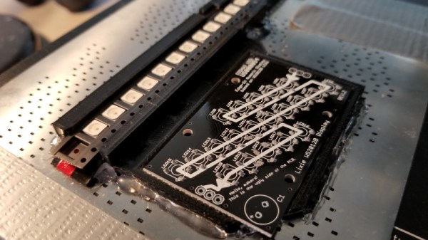
But if you have a very specific use case, namely a PCB that only has a relatively large single part that doesn’t need to be rotated, [Connor Nishijima] might have a solution for you. He bought a $150 USD Monoprice Mini, and with the addition of a few printed parts, was able to build a machine that drastically cuts down the time it takes for him to build his LED boards. Best of all the modification doesn’t involve any permanent changes to the printer, he can just pop off the vacuum attachment when he wants to print something.

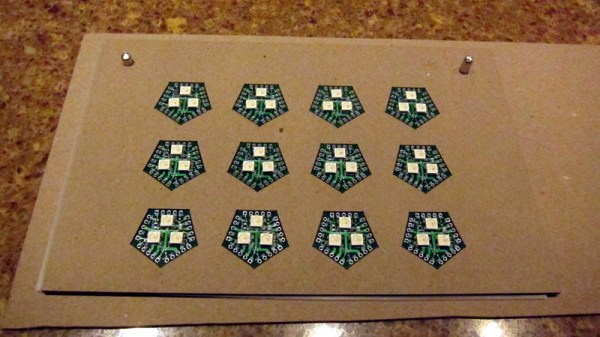
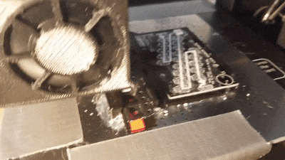
Beyond the 3D printed parts (which were made on the printer itself), the only thing you need to make the modification is the vacuum pump. [Connor] is using a hot air station that includes a vacuum pump for picking up SMD components, but he mentions that you’d probably better off just modifying an aquarium pump and using that. A printed holder snaps over the cooling fan of the Monoprice Mini to hold the vacuum pickup tool, and another printed piece holds the strip of LEDs and the PCB. It’s worth noting that the machine has no ability to control the vacuum pump, and doesn’t need to. The pickup tool is so weak that when the LED lands in the solder paste it sticks to the board well enough that the tool can’t lift it back off.

The real genius in this build comes from the manually written G-Code. You load it from the printer’s built in menu system as if it was a normal 3D print, and it instructs the printer to move the vacuum tool over the line of LEDs, pick one up, and drop it in place on the PCB. It then uses a small peg built into the vacuum tool holder to advance the line of LEDs before starting the cycle all over again. Incredibly, it does this whole complex dance 20 times for each PCB without ever having any kind of feedback or alignment check. It only works because [Connor] was willing to go through the trial and error of getting the calibration and G-Code down as close to perfect as can be expected for such a cheap machine.

This isn’t the first time we’ve seen the Monoprice Mini converted into something a bit more impressive than a cheapo 3D printer. Seems that for whatever the machine lacks in the printing department, it more than makes up for in hackability.

Continue reading “Monoprice Mini Converted To Pick And Place (Kinda)”

Acrylic Stencils Help With Component Placement For SMD Assembly

Surface mount is where the action is in the world of DIY PCBs, and deservedly so. SMDs are so much smaller than through-hole components, and fewer holes to drill make surface-mount PCBs easier to manufacture. Reflow soldering is even a snap now thanks to DIY ovens and solder stencils you can get when you order your boards.

So what’s the point of adding another stencil to the surface-mount process? These component placement stencils are [James Bowman]’s solution for speeding up assembly of boards in production runs too small to justify a pick and place robot. [James] finds that placing small components like discrete resistors and caps easy, but struggles with the placement of the larger components, like QFN packaged microcontrollers. Getting such packages lined up exactly is hard when the leads are underneath, and he found repositioning led to smeared solder paste. His acrylic stencils, which are laser-cut from SVGs derived directly from the Eagle files with a script he provides, sandwich the prepped board and let him just drop the big packages into their holes. The acrylic pops off after placement, leaving the components stuck to the solder paste and ready for their trip to the Easy Bake.

[James] claims it really speeds up hand placement in his biggish runs, and it’s a whole lot cheaper than a dedicated robot. But as slick as we think this idea is, a DIY pick and place is still really sweet.

Bandpass Filters From The CNC Mill

A bandpass allows a certain electrical signal to pass while filtering out undesirable frequencies. In a speaker bandpass, the mid-range speaker doesn’t receive tones meant for the tweeter or woofer. Most of the time, this filtering is done with capacitors to remove low frequencies and inductors to remove high frequencies. In radio, the same concept applies except the frequencies are usually much higher. [The Thought Emporium] is concerned with signals above 300MHz and in this range, a unique type of filter becomes an option. The microstrip filter ignores the typical installation of passive components and uses the copper planes of an unetched circuit board as the elements.

A nice analogy is drawn in the video, which can also be seen after the break, where the copper shapes are compared to the music tuning forks they resemble. The elegance of these filters is their simplicity, repeatability, and reproducability. In the video, they are formed on a CNC mill but any reliable PCB manufacturing process should yield beautiful results. At the size these are made, it would be possible to fit these filters on a business card or a conference badge.

Continue reading “Bandpass Filters From The CNC Mill”

Vintage Headphones Bluetooth Conversion Goes The Extra Mile

[KaZjjW] wanted to retrofit a pair of nicely styled vintage headphones to be able to play wirelessly over Bluetooth. In principle this is an easy task: simply stick a Bluetooth audio receiver on the line-in, add a battery, and you’re all set. However, [KaZjjW] wanted to keep the aesthetic changes to the headphones at an absolute minimum, retaining the existing casing and volume control, whilst cramming the electronics entirely inside and out of sight.

With the inherent space constraints inside the cups of the headphones, this proved to be quite a challenge. The existing volume potentiometer which hung half outside the case was remounted on an ingenious hinge made of two PCBs, with the pot floating next to a surface mounted switch. This allowed it to not only control the volume, but also act as an on/off switch for the Bluetooth. The only other existing cuts in the casing were a circular hole for the audio cable, and a slit for the cable strain relief. These worked perfectly for an LED status indicator and micro-USB battery charging.

The main chip used for receiving audio over Bluetooth was the BM62 by Microchip. It’s a great all-in-one solution for this kind of project as it has built-in battery charging, an on-board DAC and audio amp, as well as a serial control interface. In part 2 of the project log, the process of programming the BM62 was documented, and it was painful – it’s a shame that the software support lets it down. But a hacker will always find a way, and we’ve seen some pretty neat hacks for reprogramming existing chips in off-the-shelf Bluetooth headphones.

Two PCBs for the pot button hinge, one for the LED and micro-USB connector, as well as one for the Bluetooth receiver and a PIC. That’s four PCBs in a pretty small space, enabled by some commendable design effort both electronically and mechanically. It certainly paid off, as the finished product looks very slick.

Continue reading “Vintage Headphones Bluetooth Conversion Goes The Extra Mile”

Multi-Board Solder Stencils Explained

There was a time when reflow soldering was an impossibly exotic process at our level, something that only the most superhuman of hackers could even dream of attempting. But a demystification of the process plus the ready availability of affordable PCB and stencil manufacture has rendered into the range of almost all constructors, and it is likely that many of you reading this will have done it yourself.

Screen-printing solder paste onto a single board presents a mild alignment challenge, but how about doing it with many boards at once? [Eric Gunnerson] had this problem with a small-volume board he’s selling, and not being in the happy position of having his PCBs supplied on a panel, had to create his own multi-board alignment jig and stencil. His write-up provides a comprehensive and fascinating introduction to the process whether you are an occasional dabbler or embarking on a production run as he is.

The problem facing any would-be stenciler is that the board has to be held in place reliably in the same alignment as the stencil. With a single board, it’s easy enough to do the usual thing of taping scraps of PCB board to constrain its edges and hold it in place as a rudimentary jig, then lower the stencil onto it. Perhaps you’ve used one of those commercial stencil jigs, in which a set of magnets hold the stencil in place, or maybe you use pins to line everything up.

[Eric] takes us through the process of creating a laser-cut alignment jig for twelve boards, and cutting a matching twelve-board stencil. This includes all the software side using Inkscape, the selection of materials to match PCB thickness, and some of the issues with cutting Mylar sheet for the stencil without shrinkage at the corners. He’s using pins for alignment, and he even finds a handy supply of those in the form of shelf support pins.

We’ve visited the world of reflowing many times before. If you’d like a primer, here’s our Tools of the Trade piece on it, and if you aren’t daunted by larger projects, here’s an account of a prototype run of a significantly complex board.

How To Design Custom Shaped Boards In Fritzing

If you’re looking to get started in designing a few PCBs, you could use one of the many software packages that allow you to create a PCB quickly, easily, and with a minimum amount of fuss. You could also use Fritzing.

Fritzing is terribad and you shouldn’t use it, but that doesn’t mean you still can’t abuse Fritzing to make it do what you want. [Arduino Enigma] recently posted a tutorial on how to design custom PCB shapes for Fritzing. Yes, Fritzing is no longer limited to rectangular PCBs with sharp corners. You can make PCBs in any shape with Fritzing, provided you spend a few hours futzing about with Inkscape.

The goal for this project was to create a rectangular board without any sharp corners for [Arduino Enigma]’s Sinclair Scientific Calculator Emulator. Fritzing can make a board in the shape of a rectangle, in fact, that’s all it can do, but [Arduino Enigma] wanted a rectangle with radiused corners. After hours of work, we have the writeup on how to do it.

The imported board, with 3mm radiused corners.

The process to create a custom-shaped board, in this case, a rectangle with a 3mm radius on the corners, is simple. First, draw a rectangle of the desired shape, then draw even more rectangles as a sublayer of the current layer. Fritzing requires the layer ID to be named ‘board’, ‘silkscreen’ and ‘silkscreen0’, but this cannot be changed in Inkscape itself — you’ll need to edit the file with a text editor. After creating three layers, each containing the shape you want, simply trim the size of the page to the size of the board. Save the file, edit the file in a text editor, and click save. Launch Fritzing, load an image file, and select the SVG you’ve been working on. In just twenty or thirty quick steps, you too can import any shape you can imagine into Fritzing.

There is one pain point to this process. Editing the layer name manually with a text editor pushes this Fritzing hack from a baroque workaround into something that makes us all question the state of Open Source standards. Unfortunately, this is required because Inkscape does not use layer names as the ID in an SVG file. No, it doesn’t make sense, but that’s just the way it is.

For any other PCB design tool, creating a custom-shaped board is simply a matter of drawing a few lines. Fritzing is different, though. The top copper layer is represented as orange, and the bottom copper layer is yellow, a UI decision that doesn’t make sense, even if you aren’t colorblind. Putting more than two layers of copper on a Fritzing board is impossible. Fritzing is a tool you should avoid for PCB layout. That said, [Arduino Enigma] figured out how to do something in Fritzing that you’re not supposed to be able to do and that’s pretty cool.

Nonpareil RPN HP-41 Calculator Build

The early HP Reverse Polish Notation calculators have a special place in the hearts of engineers and tinkerers as there are lots of projects involving them. They haven’t been produced in decades, but [Chris Chung] has used some open source code to create DIY hardware version of the HP-41 Reverse Polish Notation (RPN) calculator.

The open source code behind the calculator is the Nonpareil High-Fidelity Calculator Simulator, and [Chris] has used it along with a custom designed readout and PCBs to create a working prototype. The simulator uses the original byte code of the HP-41 so the its behavior is exactly the same as the original calculator.

[Chris] has designed the PCBs so that the buttons and the screen are separate and join together. This neat idea means that he can try out different screens or different button PCBs and mix-and-match to find the combination that works best. He’s also designed a 3D printed case for the calculator. He does prefer using the bare buttons on the board to the 3D printed ones he printed for use with the case.

We love calculators here so there have been a bunch of articles over the years. Check out the documentation that comes along with this open source calculator, or check out this pocket calculator that emulates two other pocket calculators!

Continue reading “Nonpareil RPN HP-41 Calculator Build”