From what we’ve seen we’d say [Jianyi Liu] is really good at etching PCBs at home. Now you can learn from his experience. He just published a mammoth guide to fabricating your own PCBs at home. That link goes to his index page which leads to all eight parts of the guide.
He starts off by mentioning that fab house boards are rather inexpensive these days. This will save you a lot of trouble (like acquiring the equipment and raw materials needed to get up and running) but you can’t beat the turnaround time of doing it yourself.
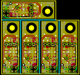
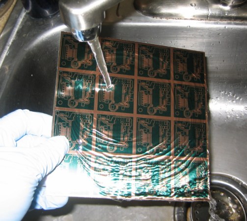
After discussing the particulars about trace width, copper thickness, and a few design considerations he lays out his board and prints the artwork to a sheet of transparency film. A pre-sensitized board is cut to size before a trip through an exposure rig with the film taped onto it. The image above shows him rinsing the board after applying the developer chemical. From here he uses cupric chloride he mixed himself to etch the board. [Jianyi] recommends populating the components before cutting the panel apart — a task which he accomplishes with a hack saw.