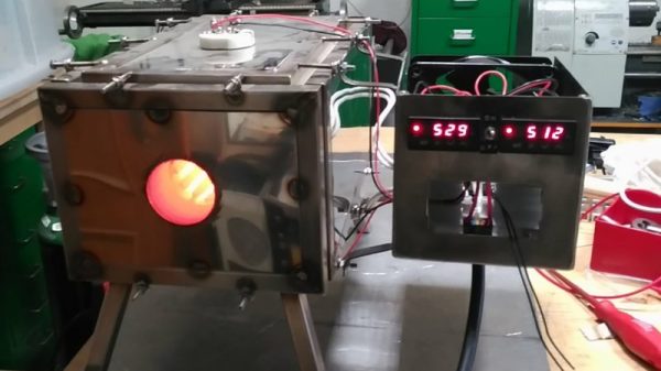
Here’s a fun exercise: take a list of the 20th century’s inventions and innovations in electronics, communications, and computing. Make sure you include everything, especially the stuff we take for granted. Now, cross off everything that can’t trace its roots back to the AT&T Corporation’s research arm, the Bell Laboratories. We’d wager heavily that the list would still contain almost everything that built the electronics age: microwave communications, data networks, cellular telephone, solar cells, Unix, and, of course, the transistor.
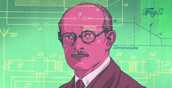
But is that last one really true? We all know the story of Bardeen, Brattain, and Shockley, the brilliant team laboring through a blizzard in 1947 to breathe life into a scrap of germanium and wires, finally unleashing the transistor upon the world for Christmas, a gift to usher us into the age of solid state electronics. It’s not so simple, though. The quest for a replacement for the vacuum tube for switching and amplification goes back to the lab of Julius Lilienfeld, the man who conceived the first field-effect transistor in the mid-1920s.
Continue reading “Julius Lilienfeld And The First Transistor”