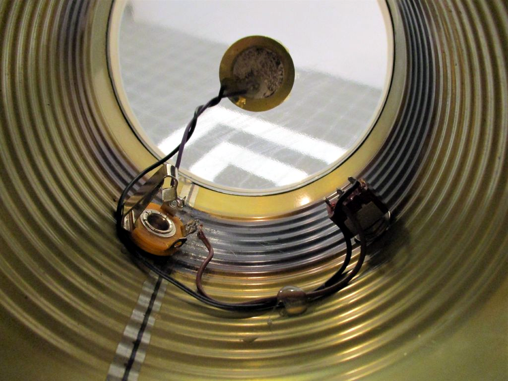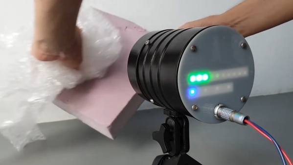
Anyone who was active in the phreaking scene or was even the least bit curious about the phone system back in the Ma Bell days no doubt remembers the carbon capsule microphone in the mouthpiece of many telephone handsets. With carbon granules sandwiched between a diaphragm and a metal plate, they were essentially sound-driven variable resistors, and they worked well enough to be the standard microphone for telephony for decades.
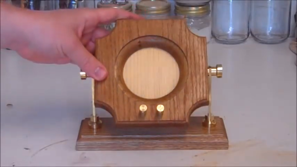
In an attempt to reduce complicated practices to their fundamentals, [Simplifier] has undertaken this surprisingly high-fidelity carbon microphone build that hearkens back to the early days of the telephone. It builds on previous work that was more proof of concept but still impressive. In both builds, the diaphragm of the microphone is a thin piece of wood, at first carved from a single block of softwood, then later improved by attaching a thin piece of pine to a red oak frame. The electrical side of the mic has four carbon rods running from the frame to the center of the diaphragm, where they articulate in a carbon block with small divots dug into it. As the diaphragm vibrates, the block exerts more or less pressure on the rods, varying the current across the mic and reproducing the sound. It works quite well, judging by the video after the break.
Congratulations to [Simplifier] for another great build and top-notch craftsmanship. We’ve seen homebrew vacuum tubes, conductive glass, and solar cells from him before, which sort of makes him the high-tech version of Primitive Technology. We’re looking forward to whatever comes next. Continue reading “Wood And Carbon Rods Used For This Handsome And Effective Microphone”