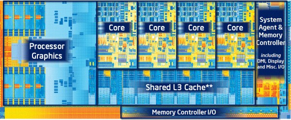
Hacklet 125 – DIY Laptops

In the old days of the 1970’s, the only way to get your own computer was to build one from scratch. Thanks to an army of hackers like [Woz], PC’s are no commodity objects that can be bought for a couple of hundred dollars. The magic of building your own still is there though – especially when we’re talking about portable machines. Laptops, notebooks, netbooks take quite a bit of skill to assemble. Stuffing a keyboard, screen, and battery into a small clamshell case takes a bit of planning. Our last look at DIY laptops was exactly 100 Hacklets ago, so it’s time for a refresh. This week we’re checking out some of the best DIY laptops and portable computers on Hackaday.io!

piberryWe start with [Sahas Dinesh Chitlange] and Pi-Berry Laptop. [Sahas] found just the right mix of simple and elegant with this build. A Raspberry Pi 2 is the brains of the operation. The Pi sits in a case built from a mix of MDF and regular wood. The display is a 10.1″ HDMI LCD. The keyboard was pulled from a tablet case. Power was easy — a USB power bank provides enough for 4-5 hours of runtime. [Sahas] covered his laptop in Italian leather for a polished look. He planned out his parts layout well enough that the power-hungry Pi stays cool without a fan.

pivenaNext up is [Tim] with PIvena. [Tim] took his inspriation from [Bunnie Huang’s] Novena open laptop. Rather than roll his own ARM board, [Tim] went with a Raspberry Pi. His original design was for the Raspberry Pi model B. Last time we looked at PIvena, the model B+ was still pretty new. As we hoped, [Tim] modified his design to accept the new Pi layouts. This means it will physically work with the B+, Pi 2, and Pi 3 boards. [Tim] didn’t stop there though. He also upgraded from an 800 x 480 LCD to an 1200 x 800 LCD. He managed to do that while keeping the same bolt pattern on the travel cover. Nice work [Tim]!

elloNext we have [KnivD] with ELLO 2M. The most striking thing about ELLO 2M is the construction. The entire laptop is made from 6 PCBs which sandwich all the other parts. The keyboard is PCB material with keys routed out. The processor is a Microchip PIC32MX470-120. Software is loaded from one of 3 microSD cards. The 7 inch touchscreen LCD and 4500 mAh LiPo battery are nestled in between PCB layers. A true hacker, [KnivD] included a generous pin grid for debugging add-on circuits. The whole setup looks great with white silkscreen. As [Mark Sherman] mentioned in the comments, this machine reminds us of a modern-day TRS-80 Model 100.

pipdaFinally we have [pdrift86] with Mini rpi2 laptop. Palmtop might be a better name for this. [pdrift86] took his inspiration (and his keyboard) from the old HP Jornada Personal Digital Assistant (PDA). The housing is Masonite, cut from a clipboard. A Raspberry Pi 2 hides inside, along with a 4 cell 18650 Li-Ion battery. The screen is a 5″ LCD with a composite input. The display isn’t a touchscreen, so a Playstation Portable analog stick is on-board, and will eventually be connected for mouse control. [pdrift86] even managed to sneak the Pi camera on the back of his machine, so it can take pictures cellphone style.

If you want to see more DIY laptop projects, check out our new DIY Laptops notebooks, and portables list. Notice a project I might have missed? Don’t be shy, just drop me a message on Hackaday.io. That’s it for this week’s Hacklet, As always, see you next week. Same hack time, same hack channel, bringing you the best of Hackaday.io!

Retro-Soviet Computer Brings The 80s Back

[Alex Zaikin] made a modern reproduction of an early-80s Soviet hobbyist home computer. Although the design was open, indeed it was published in “Radio” magazine, the project was a mammoth undertaking involving around 200 microchips, so not many “Mikro-80” computers were actually made.

[Alex] wanted to simplify the project and reduce the parts count. These days, 200 microchips’ worth of logic can easily fit inside an FPGA, and [Alex] wrangled the chip count down to seven. Moreover, he made it even easier to build your own retro minicomputer by building a modular platform: Retrobyte.

With the Retrobyte providing all of the essential infrastructure — SD card, tape recorder I/O, VGA outputs, and more — and the FPGA providing the brains, all that was left was to design a period keyboard and 3D print a nice enclosure. Project complete! Time for a few rounds of ASCII Tetris to celebrate.

We’ve covered a number of retro computer projects. We just have a soft spot for them, is all. If you don’t know what all the fuss is about, you could start out with a kit build to get your feet wet. Before long, you’ll be emulating ever obscurer computers of yore in custom logic. And when you do, be sure to drop us a line!

Review: The RC2014 Z80 Computer

As hackers and makers we are surrounded by accessible computing in an astonishing diversity. From tiny microcontrollers to multi-processor powerhouses, they have become the universal tool of our art. If you consider their architecture though you come to a surprising realisation. It is rare these days to interface directly to a microprocessor bus. Microcontrollers and systems-on-chip have all the functions that were once separate peripherals integrated into their packages, and though larger machines such as your laptop or server have their processor bus exposed you will never touch them as they head into your motherboard’s chipset.

A few decades ago this was definitely not the case. A typical 8-bit microprocessor of the 1970s had an 8-bit data bus, a 16-bit address bus, and a couple of request lines to indicate whether it wanted to talk to memory or an I/O port. Every peripheral you connected to it had to have some logic to decode its address and select it when you wanted to use it, and all shared the processor’s bus. This was how those of us whose first computers were the 8-bit machines of the late 1970s and early 1980s learned the craft of computer hardware, and in a world of Arduino and Raspberry Pi this now seems a lost art.

The subject of today’s review then provides a rare opportunity for the curious hardware hacker to get to grips with a traditional microprocessor bus. The RC2014 is a modular 8-bit computer in which daughter cards containing RAM, ROM, serial interface, clock, and Z80 processor are ranged on a backplane board, allowing complete understanding of and access to the workings of each part of the system. It comes with a ROM BASIC, and interfaces to a host computer through a serial port. There is also an ever-expanding range of further peripheral cards, including ones for digital I/O, LED matrixes, blinkenlights, a Raspberry Pi Zero for use as a VDU, and a small keyboard.

Continue reading “Review: The RC2014 Z80 Computer”

Atari Archaeology Without Digging Up Landfill Sites

We are fortunate to live in an age of commoditized high-power computer hardware and driver abstraction, in which most up-to-date computers have the ability to do more or less anything that requires keeping up with the attention of a human without breaking a sweat. Processors are very fast, memory is plentiful, and 3D graphics acceleration is both speedy and ubiquitous.

Thirty years ago it was a different matter on the desktop. Even the fastest processors of the day would struggle to perform on their own all the tasks demanded of them by a 1980s teenager who had gained a taste for arcade games. The manufacturers rose to this challenge by surrounding whichever CPU they had chosen with custom co-processors, ASICs that would take away the heavy lifting associated with 2D graphics acceleration, or audio and music synthesis.

One of the 1980s objects of computing desire was the Atari ST, featuring a Motorola 68000 processor, a then-astounding 512k of RAM, a GUI OS, high-res colour graphics, and 3.5″ floppy drive storage. Were you to open up the case of your ST you’d have found those ASICs we mentioned as being responsible for its impressive spec.

Jumping forward three decades, [Christian Zietz] found that there was frustratingly little information on the ST ASIC internal workings. Since a trove of backed-up data became available when Atari closed down he thought it would be worth digging through it to see what he could find. His write-up is a story of detective work in ancient OS and backup software archaeology, but it paid off as he found schematics for not only an ASIC from an unreleased Atari product but for the early ST ASICs he was looking for. He found hundreds of pages of schematics and timing diagrams which will surely take the efforts of many Atari enthusiasts to fully understand, and best of all he thinks there are more to be unlocked.

We’ve covered a lot of Atari stories over the years, but many of them have related to their other products such as the iconic 2600 console. We have brought you news of an open-source ST on an FPGA though, and more recently the restoration of an ST that had had a hard life. The title of this piece refers to the fate of Atari’s huge unsold stocks of 2600 console cartridges, such a disastrous marketing failure that unsold cartridges were taken to a New Mexico landfill site in 1983 and buried. We reported on the 2013 exhumation of these video gaming relics.

A tip of the hat to Hacker News for bringing this to our attention.

Atari ST image, Bill Bertram (CC-BY-2.5) via Wikimedia Commons.

Colossus: Face To Face With The First Electronic Computer

When the story of an invention is repeated as Received Opinion for the younger generation it is so often presented as a single one-off event, with a named inventor. Before the event there was no invention, then as if by magic it was there. That apple falling on Isaac Newton’s head, or Archimedes overflowing his bath, you’ve heard the stories. The inventor’s name will sometimes differ depending on which country you are in when you hear the story, which provides an insight into the flaws in the simple invention tales. The truth is in so many cases an invention does not have a single Eureka moment, instead the named inventor builds on the work of so many others who have gone before and is the lucky engineer or scientist whose ideas result in the magic breakthrough before anyone else’s.

The history of computing is no exception, with many steps along the path that has given us the devices we rely on for so much today. Blaise Pascal’s 17th century French mechanical calculator, Charles Babbage and Ada, Countess Lovelace’s work in 19th century Britain, Herman Hollerith’s American tabulators at the end of that century, or Konrad Zuse’s work in prewar Germany represent just a few of them.

So if we are to search for an inventor in this field we have to be a little more specific than “Who invented the first computer?”, because there are so many candidates. If we restrict the question to “Who invented the first programmable electronic digital computer?” we have a much simpler answer, because we have ample evidence of the machine in question. The Received Opinion answer is therefore “The first programmable electronic digital computer was Colossus, invented at Bletchley Park in World War Two by Alan Turing to break the Nazi Enigma codes, and it was kept secret until the 1970s”.

It’s such a temptingly perfect soundbite laden with pluck and derring-do that could so easily be taken from a 1950s Eagle comic, isn’t it. Unfortunately it contains such significant untruths as to be rendered useless. Colossus is the computer you are looking for, it was developed in World War Two and kept secret for many years afterwards, but the rest of the Received Opinion answer is false. It wasn’t invented at Bletchley, its job was not the Enigma work, and most surprisingly Alan Turing’s direct involvement was only peripheral. The real story is much more interesting.

Continue reading “Colossus: Face To Face With The First Electronic Computer”

A PDP-11 On A Chip

If you entered the world of professional computing sometime in the 1960s or 1970s there is a high probability that you would have found yourself working on a minicomputer. These were a class of computer smaller than the colossal mainframes of the day, with a price tag that put them within the range of medium-sized companies and institutions rather than large corporations or government-funded entities. Physically they were not small machines, but compared to the mainframes they did not require a special building to house them, or a high-power electrical supply.

A PDP-11 at The National Museum Of Computing, Bletchley, UK.

One of the most prominent among the suppliers of minicomputers was Digital Equipment Corporation, otherwise known as DEC. Their PDP line of machines dominated the market, and can be found in the ancestry of many of the things we take for granted today. The first UNIX development in 1969 for instance was performed on a DEC PDP-7.

DEC’s flagship product line of the 1970s was the 16-bit PDP-11 series, launched in 1970 and continuing in production until sometime in the late 1990s. Huge numbers of these machines were sold, and it is likely that nearly all adults reading this have at some time or other encountered one at work even if we are unaware that the supermarket till receipt, invoice, or doctor’s appointment slip in our hand was processed on it.

During that over-20-year lifespan of course DEC did not retain the 74 logic based architecture of the earliest model. Successive PDP-11 generations featured ever greater integration of their processor, culminating by the 1980s in the J-11, a CMOS microprocessor implementation of a PDP-11/70. This took the form of two integrated circuits mounted on a large 60-pin DIP ceramic wafer. It was one of these devices that came the way of [bhilpert], and instead of retaining it as a curio he decided to see if he could make it work.

The PDP-11 processors had a useful feature: a debugging console built into their hardware. This means that it should be a relatively simple task to bring up a PDP-11 processor like the J-11 without providing the rest of the PDP-11 to support it, and it was this task that he set about performing. Providing a 6402 UART at the address expected of the console with a bit of 74 glue logic, a bit more 74 for an address latch, and a couple of  6264 8K by 8 RAM chips gave him a very simple but functional PDP-11 on a breadboard. He found it would run with a clock speed as high as 11MHz, but baulked at a 14MHz crystal. He suggests that the breadboard layout may be responsible for this. Hand-keying a couple of test programs, he was able to demonstrate it working.

We’ve seen a lot of the PDP-11 on these pages over the years. Of note are a restoration of a PDP-11/04, this faithful reproduction of a PDP-11 panel emulated with the help of a Raspberry Pi, and an entire PDP-11 emulated on an AVR microcontroller. We have indeed come a long way.

Thanks [BigEd] for the tip.

[Ken Shirriff] Demystifies BeagleBone I/O

If you have ever spent a while delving into the bare metal of talking to the I/O pins on a contemporary microprocessor or microcontroller you will know that it is not always an exercise for the faint-hearted. A host of different functions can be multiplexed behind a physical pin, and once you are looking at the hardware through the cloak of an operating system your careful timing can be derailed in an instant. For these reasons most of us will take advantage of other people’s work and use the abstraction provided by a library or a virtual filesystem path.

If you have ever been curious enough to peer under the hood of your board’s I/O then you may find [Ken Shirriff]’s latest blog post in which he explores the software stack behind the pins on a BeagleBone Black to be of interest. Though its specifics are those of one device, the points it makes have relevance to many other similar boards.

He first takes a look at the simplest way to access a Beagle Bone’s I/O lines, through virtual filesystem paths. He then explains why relying so heavily on the operating system in this way causes significant timing issues, and goes on to explore the physical registers that lie behind the pins. He then discusses the multiplexing of different pin functions before explaining the role of the Linux device tree in keeping operating system in touch with hardware.

For some Hackaday readers this will all be old news, but it’s safe to say that many users of boards like the BeagleBone Black will never have taken a look beyond the safely abstracted ways to use the I/O pins. This piece should therefore provide an interesting education to the chip-hardware novice, and should probably still contain a few nuggets for more advanced users.

We’ve seen a lot of [Ken]’s work here at Hackaday over the years, mostly in the field of reverse engineering. A few picks are his explanation of the TL431 voltage reference, a complete examination of the 741 op-amp, and his reverse engineering of the 1970s Sinclair Scientific calculator.

We appreciate [Fustini]’s tip on this story.

BeagleBone Black image: BeagleBoard.org Foundation [CC BY-SA 3.0], via Wikimedia Commons.