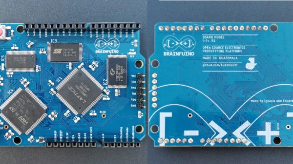
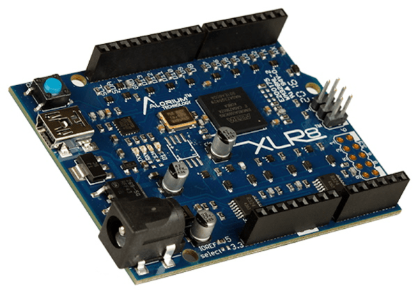
What’s Inside An FPGA? Ken Shirriff Has (Again) The Answer

FPGAs are somewhat the IPv6 of integrated circuits — they’ve been around longer than you might think, they let you do awesome things that people are intrigued by initially, but they’ve never really broke out of their niches until rather recently. There’s still a bit of a myth and mystery surrounding them, and as with any technology that has grown vastly in complexity over the years, it’s sometimes best to go back to its very beginning in order to understand it. Well, who’d be better at taking an extra close look at a chip than [Ken Shirriff], so in his latest endeavor, he reverse engineered the very first FPGA known to the world: the Xilinx XC2064.

If you ever wished for a breadboard-friendly FPGA, the XC2064 can scratch that itch, although with its modest 64 configurable logic blocks, there isn’t all that much else it can do — certainly not compared to even the smallest and cheapest of its modern successors. And that’s the beauty of this chip as a reverse engineering target, there’s nothing else than the core essence of an FPGA. After introducing the general concepts of FPGAs, [Ken] (who isn’t known to be too shy to decap a chip in order to look inside) continued in known manner with die pictures in order to map the internal components’ schematics to the actual silicon and to make sense of it all. His ultimate goal: to fully understand and dissect the XC2064’s bitstream.

Of course, reverse engineering FPGA bitstreams isn’t new, and with little doubt, building a toolchain based on its results helped to put Lattice on the map in the maker community (which they didn’t seem to value at first, but still soon enough). We probably won’t see the same happening for Xilinx, but who knows what [Ken]’s up to next, and what others will make of this.

Write In PipelineC For FPGAs

The best thing about field-programmable gate arrays (FPGAs), when you have a massively parallel application, is that everything runs in parallel. The worst thing about FPGAs, when you need a lot of stuff to happen in sequence, is that everything runs in parallel. If you have a multi-step computation, for example, you need to break it up into chunks, figure out the timing between them, and make sure that each chunk clears before it is fed new data. This is pipelining, and taking care of all the low-level details yourself is one of the things that can sometimes make FPGA a four-letter word beginning with “F”.

[Julian Kemmerer]’s PipelineC is a C-like language that compiles down into VHDL so that you can use it in an FPGA, and it does the pipelining for you. He has examples of how you’d use it to construct a simple state machine, and after you’ve written a few hundred state machines the long way, you’ll know why this is a good idea.

PipelineC isn’t the only high level synthesis language out there, but it sits in an interesting place. It doesn’t take care of memory or define interfaces. It just takes care of pipelining. We haven’t tried it out yet, but it looks like it would be interesting for moderately complex projects, where the mechanics of pipeline signalling is a hassle, but you don’t require the deluxe treatment. Check it out, and if you like it, let us (and [Julian], natch) know.

If you want to dive head-first into pipelining, give [Al Williams]’ two-part mini-series a look.

Pipeline graphic CC BY-SA 3.0 by CBurnett

Glasgow Uses An FPGA As An Embedded Systems Multitool

Everyone who builds embedded systems wants tools to help build and debug systems faster, so it isn’t uncommon to see boards outfitted with various tools like serial port sniffers. We’ve seen a few incarnations and the latest is Glasgow. The small board uses an FPGA and claims to do the following:

  • UART with automatic baud rate determination
  • SPI or I2C
  • Read and write common EEPROMs and flash chips
  • Read and write common EPROMs including a data rescue function
  • Program AVR chips via SPI
  • Play back JTAG SVF files
  • Debug ARC and some MIPS CPUs
  • Program XC9500LX CPLDs
  • Communicate to several wireless radios and CPUs
  • Do sound synthesis
  • Read raw data from floppy drives

The revC board is the first to be relatively functional and sports 16 I/O pins operating at up to 100 MHz, although the documentation hints that 6 MHz might be the top of what’s easily accomplished. The software is written in Python and the iCE40 FPGA toolchain that we’ve talked about many times in the past.

This already looks like a useful tool and the reconfigurable nature of FPGAs makes it a good platform to expand. The documentation discusses the difficulty in debugging things for the board, so the base software offers support such as a built-in logic analyzer to help.

We have seen dev boards become bench tools, like using the iCEstick as a logic analyzer. It’s nice to see dedicated tools like this one built up around the speed and versatility of FPGAs.

Continue reading “Glasgow Uses An FPGA As An Embedded Systems Multitool”

SoftCore CPU Comparison

Monty Python once did a sketch where people tried to summarize Proust in fifteen seconds. Although summarizing eight FPGA-based CPUs is almost as daunting, [jaeblog] does a nice job of giving a quick sketch of how the CPUs work with the Xilinx Vivado toolchain and the Digilent Arty board.

The eight CPUs are:   VexRiscv, LEON3, PicoRV32, Neo430, ZPU, Microwatt, S1 Core, and Swerv EH1.

The comparison criteria were very practical: A C compiler (gcc or llvm) for each CPU and no CPUs that were tied to a particular FPGA. Two of the CPUs didn’t fit on the Arty board, so their comparisons are a bit more theoretical.  There were other considerations such as speed, documentation, debugging support, and others.

It was interesting to see the various CPUs ranging from some very mature processors to some new kids on the block, and while the evaluations were somewhat subjective, they seemed fair and representative of the things you’d look for yourself. You can also get the test code if you want to try things for yourself.

The winner? The post identifies three CPUs that were probably the top choices, although none were just perfect. Of course, your experience may vary.

If you want an easy introduction to adding things to a soft CPU, this RISC-V project is approachable. Or if you prefer SPARC, check out this project.

The Cheap Way To Glitch An STM8 Microcontroller

Reverse engineering or modifying a device often requires you to access the firmware stored on a microcontroller. Since companies are usually not fond of people who try to peek into their proprietary data, most commercial devices are readout protected. [rumpeltux] ran into this problem when he tried to dump the firmware on an HC-12 wireless serial communication module for yet undisclosed reasons. Hacking into the device was a challenge that he gladly accepted and in the end, he succeeded by building a low-cost setup for voltage glitching.

Voltage glitching is a form of fault injection that has, e.g., been successfully used to hack the Playstation Vita. It involves the injection of voltage spikes on the power line in order to force the bootloader to skip security checks. The hard thing is trying to find the right shape of the waveform and the best way to inject the signal.

While there are already open-source boards for fault injection like ChipWhisperer, [rumpeltux] chose to build his own setup around an FPGA. By using a cheap EPM240 board, some MOSFET, and a USB-to-Serial converter, the total costs of the glitching setup were under 20 Euros. [rumpeltux] then recorded a larger number of voltage traces on the VCC pin around the reset phase and analyzed the differences. This helped him to pinpoint the best time for injecting the signal and refine the search space. After some unsuccessful attempts to glitch the VCC and GND pins, he got lucky when using one of the voltage regulator pins instead.

Be sure not to miss Samy Kamkar’s talk at Supercon 2019 if you want to know more about hardware attacks or how to eavesdrop on people using a bag of potato chips.

Your Own Open Source ASIC: SkyWater-PDK Plans First 130 Nm Wafer In 2020

You might have caught Maya Posch’s article about the first open-source ASIC tools from Google and SkyWater Technology. It envisions increased access to make custom chips — Application Specific Integrated Circuits — designed using open-source tools, and made real through existing chip fabrication facilities. My first thought? How much does it cost to tape out? That is, how do I take the design on my screen and get actual parts in my hands? I asked Google’s Tim Ansel to explain some more about the project’s goals and how I was going to get my parts.

The goals are pretty straightforward. Tim and his collaborators would like to see hardware open up in the same way software has. The model where teams of people build on each other’s work either in direct collaboration or indirectly has led to many very powerful pieces of software. Tim’s had some success getting people interested in FPGA development and helped produce open tools for doing so. Custom ASICs are the next logical step.

Continue reading “Your Own Open Source ASIC: SkyWater-PDK Plans First 130 Nm Wafer In 2020”

Xilinx Makes MIPI CSI And DSI Controller IP Blocks Free To Use With Vivado

If you want to use a display or camera with an FPGA, you will often end up with a MIPI-based solution. As of the Xilinx Vivado 2020.1 release, the MIPI DSI (display serial interface) and CSI (camera serial interface) IP blocks are now bundled with the IDE to be used freely with Xilinx FPGAs.

The Xilinx MIPI CSI2 receiver block implements the CSI-2 v1.1 specification, which although a bit older is essentially the same CSI implementation as on the Raspberry Pi boards. This means that it would allow one to use this IP block on an FPGA with many common CSI camera modules out there. The IP block offers a standard AXI4 interface for connecting up to the rest of a design.

Similarly, the Xilinx MIPI DSI transmitter block implements DSI v1.3 specification. This offers a maximum data rate of 1.5 Gbps, with an AXI4-lite interface to communicate with the rest of the design. Both IP blocks are subject to the Core license agreement, which doesn’t appear to preclude it from being used in a specific fashion, whether commercial or personal.

This is not the only way to use MIPI devices with an FPGA, of course. Take for example [Daveshah]’s CSRIx project on Github.

Header image: Kwapix / CC BY-SA 4.0