When used for cracking passwords, a modern high-end graphics card will absolutely chew through “classic” hashing algorithms like SHA-1 and SHA-2. When a single desktop machine can run through 50+ billion password combinations per second, even decent passwords can be guessed in a worryingly short amount of time. Luckily, advanced password hashing functions such as bcrypt are designed specifically to make these sort of brute-force attacks impractically slow.
Cracking bcrypt on desktop hardware might be out of the question, but the folks over at [Scattered Secrets] had a hunch that an array of FPGAs might be up to the task. While the clock speed on these programmable chips might seem low compared to a modern CPUs and GPUs, they don’t have all that burdensome overhead to contend with. This makes the dedicated circuitry in the FPGA many times more efficient at performing the same task. Using a decade-old FPGA board intended for mining cryptocurrency, the team was able to demonstrate a four-fold performance improvement over the latest generation of GPUs.
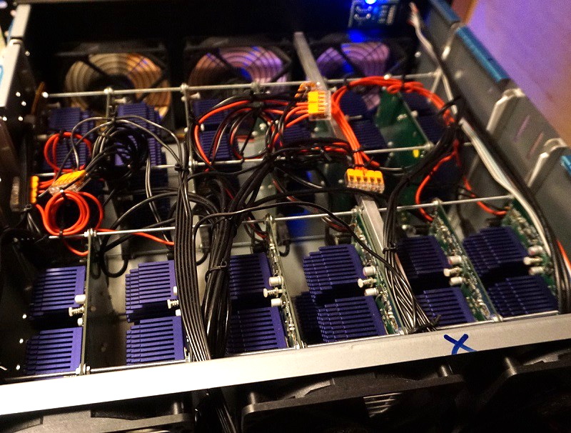
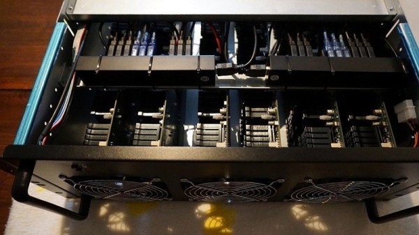
After seeing what a single quad FPGA board was capable of, the [Scattered Secrets] team started scaling the concept up. The first version of the hardware crammed a dozen of the ZTEX FPGA boards and a master control computer computer into a standard 4U server case. For the second version, they bumped that up to 18 boards for a total of 72 FPGAs, and made incremental improvements to the power and connectivity systems.
Each 4U FPGA cracker is capable of 2.1 million bcrypt hashes per second, while consuming just 585 watts. To put that into perspective, [Scattered Secrets] says you’d need at least 75 Nvidia RTX-2080Ti graphics cards to match that performance. Such an array would not only take up a whole server rack, but would burn through a staggering 25 kilowatts. Now might be a good time to change your password to something longer, or finally get onboard with 2FA.
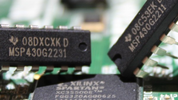
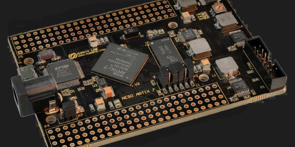
We’ve covered attempts to reverse engineer hardware designed for cryptocurrency mining, but those were based around application-specific integrated circuits (ASICs) which by definition are very difficult to repurpose. On the other hand, disused FPGA-based miners offer tantalizing possibilities; once you wrap your mind around how they work, anyway.
[Thanks to Piejoe for the tip.]

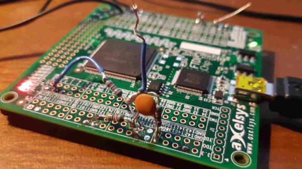
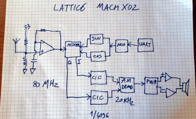 He describes it as an SDR, which given that it’s created from Verilog, is a term that could be applied to it. But instead of using an SDR topology of ADC and digital signal processing, it implements a surprisingly traditional direct conversion receiver.


