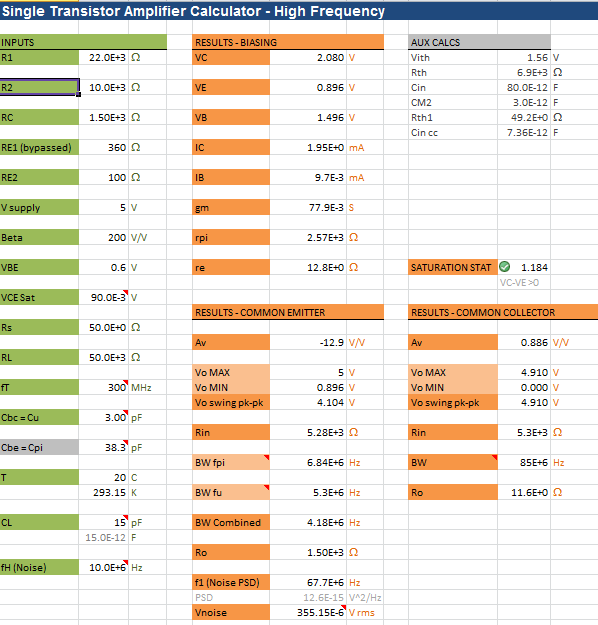
[Paulo] just tipped us about an Excel based high frequency transistor amplifier calculator he made. We’re guessing that some of our readers already are familiar with these class A amplifiers, commonly used to amplify small audio signals. Skipping over the fact that their efficiency is quite low — they are cheap to make, don’t require many components and usually are a great way to introduce transistors to new electronics enthusiasts. All you usually need to do is a few calculations to properly set your output signals and you’re good to go.
Things are however more complex when you are amplifying 200MHz+ signals, as all the components (complex) impedances have to be taken into account so you can get a nice amplification system. On a side note, at these frequencies your transmission lines impedances may even vary depending on how much solder and flux you left on your SMT pads along the way. [Paulo]’s calculator will therefore compute most of the characteristics of two class A common emitter/collector amplifiers for specified loads.
 Flappy Bird has been ported to just about every system imaginable, including but not limited to the Apple II, Commodores, pretty much every version of the Atari, and serves as a really great demonstration of the TI-99’s graphics capabilities. Porting is one thing, but having a computer automate Flappy Bird is another thing entirely. [Ankur], [Sai], and [Ackerly] in [Dr. Bruce Land]’s advanced microcontroller design class at Cornell
  ng
ng

 There’s a problem with products geared towards building the Internet of Things. Everyone building hardware needs investors, and thus some way to monetize their platform. This means all your data is pushed to ‘the cloud’, i.e. a server you don’t own. This is obviously not ideal for the Hackaday crowd. Yes, IoT can be done with a few cheap radios and a hacked router, but then you don’t get all the cool features of a real Things project – mesh networking and a well designed network.