Making A Solid-state Relay With I2C Interface

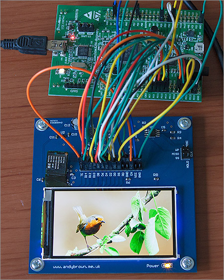
As [Mic] often got requests to make high-power switching boards, he recently finally gave in and designed the one shown above based around a solid-state relay. Some of our readers that already play with mains power know that switching should normally occur when the voltage crosses zero volts. The ‘TRIAC BLOC’ is able to do so, which also allows mains frequency measurement. [Mic] then tuned to the internal oscillator of his ATtiny microcontroller with this 50Hz by adjusting its OSCCAL register value, so the switching command can be sent at the ideal moment. Zero crossing detection is implemented by feeding the mains into an AC optocoupler. [Mic] discovered that the optocoupler diodes are not identical, so he had to adjust his firmware to account for the time differences.

All the resources are available on github, we would be interested to hear your detailed analysis of the circuit implemented with the passives R3/C1/L1/R8/C3.

Hackaday Interview With Amal Graafstra, Creator Of XNT Implant Chip

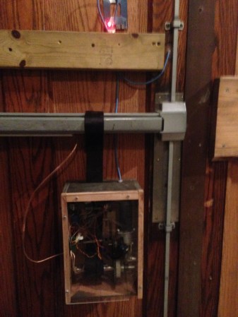
Near Field Communication (NFC) enabled devices are starting to appear in our everyday lives. Shown in the picture above is the xNT (fundraiser warning), a 2mm x 12mm fully NFC Type 2 compliant 13.56MHz RFID tag encased in a cylindrical Schott 8625 bioglass ampule. It was created by [Amal Graafstra], who therefore aims to produce the world’s first NFC compliant RFID implant. The chip used is the NTAG203, which is (for the sake of simplicity) a 144bytes EEPROM with different protection features.

We can only start thinking of the different possibilities this chip will create in the near future, but also wonder which precedent this may set for future NFC enabled humans. Embedded after the break is the presentation video of xNT but also an interview I conducted with [Amal Graafstra], who has already been living for 8 years with RFID tags in each hand.

Continue reading “Hackaday Interview With Amal Graafstra, Creator Of XNT Implant Chip”

Weightless, The Internet Of Things Chip, Becomes Less Vaporware

weightless

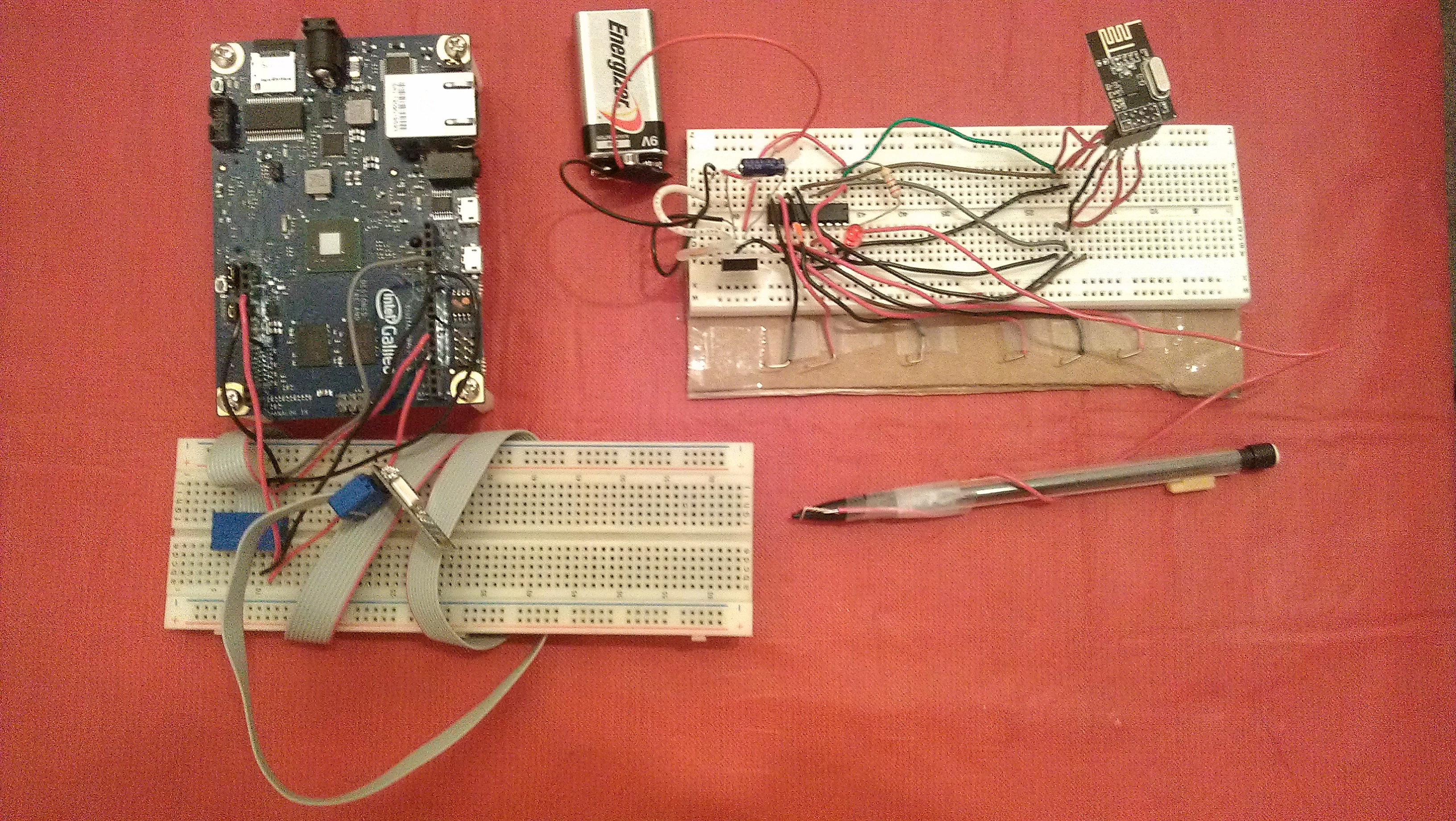
Several months ago, we caught wind of Weightless, a $2 chip that will run for 10 years on a AA battery and communicate to a Weightless base station 10 Km away. Yes, this is the fabled Internet of Things chip that will allow sensors of every type to communicate with servers around the world. It looks like Weightless is becoming less and less vaporware, as evidenced by the Weightless SIG hardware roadmap; Weightless modules might be in the hands of makers and designers in just a few short months.

Weightless is an extremely low-cost wireless module that operates in the radio spectrum previously occupied by analog broadcast television. This is a great place for the Internet of Things, as signals in this spectrum have a lot of range and the ability to go through walls. These signals are sent to a Weightless base station where they are then sent over the Internet to servers around the world.

The Weightless SIG has been hard at work producing new silicon, with the third generation of chips heading for volume production next month. The only thing this chip requires is a battery and an antenna, making Weightless integration for new designs and projects a snap.

There’s one thing Weightless is not, and that’s a free, high-speed connection to the Internet with a $2 adapter. Weightless is designed for sensors that only transmit a kilobyte or so a day – medical sensors, irrigation control, and other relatively boring things. There’s a summary video from the recent 2013 Weightless SIG Summit going over all this information below.

Continue reading “Weightless, The Internet Of Things Chip, Becomes Less Vaporware”

Easy-phi: An Open Source Platform For Experimenters

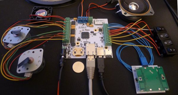
As a few of Hackaday readers may already know, my day job involves working with high speed electronics. For the last few months, my team at [Université de Genève] in Switzerland has been working on an open source platform (mostly) targeted for experimenters: the easy-phi project. The main idea is to build a simple, cheap but intelligent open hardware/software platform consisting of a 19″ frame (or smaller), which can house a big variety of electronic modules. Hobbyist would therefore only make/buy the modules that would suit their needs and control them through a web page / standalone application / Labview module.

I detailed in more depth on my website the technical aspects of the project. To give you a quick and simple overview, the rack is essentially a USB hub that connects all the modules to a Cubieboard. It also integrates a few synchronization signals, a clock and a monitoring system for voltages, temperatures, power consumption. The modules are made of template + module specific electronics. The template electronics are part of the ‘easy-phi standard’, they consist of the Arduino compatible SAM3X8E microcontroller and of a few other power related components. This ensures electrical and firmware compatibility between the rack and modules that you guys may develop. It is important to note that the modules are enumerated on the USB bus as composite CDC (communication device) and MSC (mass storage). The CDC is used to configure the module while the MSC allows you to grab its documentation, resources, and standalone application in case you use the module without the rack.

The chosen schematics / layout software is Kicad, and all current files can be found on our github. Others will be uploaded once we have tested the other modules currently in the pipe. As the ones we’re developing are physics oriented, we hope that enthusiasts will bring easy-phi to other domains. Don’t hesitate to contact us if you have any question or if you’d like to contribute.

Woodcut Stamps And Conductive Ink

circuit

Even though it’s been a while since the Rome Maker Faire, we’re still getting some tips from the trenches of Europe’s largest gathering of makers. One of these is a 30-minute experiment from [Luong]. He wondered if it would be possible to create SMD circuit boards by using a 3D printer to fabricate a stamp for conductive ink.

[Luong] told this idea  to a few folks around the faire, and the idea eventually wound up in the laps of the guys from TechLab. the Chieri, Italy hackerspace. They suggested cutting a wooden stamp using a laser cutter and within 30 minutes of the idea’s inception a completed stamp for an Atari Punk Console PCB was in [Luong]’s hands.

As an experiment, the idea was a tremendous success. As a tool, the stamp didn’t perform as well as hoped; the traces didn’t transfer properly, and there’s no way this wooden laser cut stamp could ever create usable PCBs.

That being said, we’re thinking [Luong] is on the right track here with printed PCBs. One of the holy grails of home fabrication is the creation of printed circuit boards, and even a partial success is too big to ignore.

This idea for CNC-created PCB stamps might work with a different material – linoleum or other rubber stamp material, or even a CNC milled aluminum plate. If you have any ideas on how to use this technique for PCB creation, leave a note in the comments, or better yet, try it out for yourself.

Making A Diode Matrix ROM

Here is a nice project that allows youngsters (but also adults!) to actually see the data stored in a Read Only Memory (ROM). The memory shown in the picture above is made of diodes. [Scott] made it as a part of his Barcamp Fall 2013 presentation about visualizing ROMs. He starts his write-up by stating the obvious: this memory is not practical. Nonetheless, it still was a fun exercise to do. [Scott] then greatly described all the different kinds of read only memories that you can find out there, with a few words explaining how they work. In his diode ROM, bits are ‘programmed’ by adding (or not) a diode between a given data line (anode) and an address line (cathode). When pulling low a given address line, the corresponding data line will only be pulled low if a diode is present. [Scott] finally checked his circuit by using a very old device programmer which could only be run in DOS.

An Open Source GPU

Unless you’re bit-banging a CRT interface or using a bunch of resistors to connect a VGA monitor to your project, odds are you’re using proprietary hardware as a graphics engine. The GPU on the Raspberry Pi is locked up under an NDA, and the dream of an open source graphics processor has yet to be realized. [Frank Bruno] at Silicon Spectrum thinks he has the solution to that: a completely open source GPU implemented on an FPGA.

Right now, [Frank] has a very lightweight 2D and 3D engine well-suited for everything from servers to embedded devices. If their Kickstarter meets its goal, they’ll release their project to the world, giving every developer and hardware hacker out there a complete, fully functional, open source GPU.

Given the difficulties [Bunnie] had finding a GPU that doesn’t require an NDA to develop for, we’re thinking this is an awesome project that gets away from the closed-source binary blobs found on the Raspberry Pi and other ARM dev boards.