Open Source Intel Helps Reveal US Spy Sat Capabilities

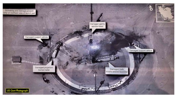
On the 30th August 2019, the President of the United States tweeted an image of an Iranian spaceport, making note of the recent failed Safir launch at the site. The release of such an image prompted raised eyebrows, given the high resolution of the image, and that it appeared to be a smartphone photo taken of a classified intelligence document.

Inquisitive minds quickly leapt on the photo, seeking to determine the source of the image. While some speculated that it may have been taken from a surveillance aircraft or drone, analysis by the satellite tracking community disagreed.

A comparison of the actual image, top, and a simulation of what a shot from USA 224 would look like. Ignore the shadows, which are from an image taken at a different time of day. Note the very similar orientation of the features of the launchpad.

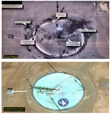
The angle of shadows in the image was used to determine the approximate time that the image was taken. Additionally, through careful comparison with existing satellite images from Google Maps, it was possible to infer the azimuth and elevation of the camera. Positions of military satellites aren’t made public, but amateur tracking networks had data placing satellite USA 224 at a similar azimuth and elevation around the time the image was taken.

With both the timing and positioning pointing to USA 224, evidence seems conclusive that this KH-11 satellite was responsible for taking the image. The last confirmed public leak of a Keyhole surveillance image was in 1984, making this an especially rare occurrence. Such leaks are often frowned upon in the intelligence community, as nation states prefer to keep surveillance capabilities close to their chest. The Safir images suggest that USA 224 has a resolution of 10cm per pixel or better – information that could prove useful to other intelligence organisations.

It’s not the first time we’ve covered formerly classified information, either – this teardown of a Soviet missile seeker bore many secrets.

RISC-V Uses Carbon Nanotubes

In a recent article in Nature, you can find the details of a RISC-V CPU built using carbon nanotubes. Of course, Nature is a pricey proposition, but you can probably find the paper by its DOI number if you bother to look for it. The researchers point out that silicon transistors are rapidly reaching a point of diminishing returns. However, Carbon Nanotube Field Effect Transistors (CNFETs) overcome many of these disadvantages.

The disadvantage is that the fabrication of CNFETs has been somewhat elusive. The tubes tend to clump and yields are low. The paper describes a method that allowed the fabrication of a CPU with over 14,000 transistors. A wafer gets nanotubes grown all over it and then some of them are removed. In addition, some design rules mitigate other problems.

In particular, a small percentage of the CNFETs will become metallic and have little to no bandgap. However, the DREAM design rules can increase the tolerance of the design to metallic CNFETs with no process changes.

Before you get too excited, limitations in channel length and contact size keep the processor running at a blazing 10 kHz. To paraphrase Weird Al, your operating system boots in a day and a half. The density isn’t great either since working around stray and metallic CNFETs means each transistor has multiple nanotubes in use.

On the other hand, it works. New technology doesn’t always match old technology at first, but you have to crawl before you walk, and walk before you run.

We imagine you won’t be able to buy this for $8 any time soon even if you wanted to. At 10 kHz, it probably isn’t going to make much of a desktop PC anyway.

A Radio Transceiver From A Cable Modem Chipset

It’s a staple of our community’s work, to make electronic devices do things their manufacturers never intended for them. Analogue synthesisers using CMOS logic chips for example, or microcontrollers that bitbang Ethernet packets without MAC hardware. One of the most fascinating corners of this field comes in the form of software defined radios (SDRs), with few of us not owning an RTL2832-based digital TV receiver repurposed as an SDR receiver.

The RTL SDR is not the only such example though, for there is an entire class of cable modem chipsets that contain the essential SDR building blocks. The Hermes-Lite is an HF amateur radio transceiver project that uses an AD9866 cable modem chip as the signal end for its 12-bit SDR transceiver hardware with an FPGA between it and an Ethernet interface. It covers frequencies from 0 to 38.4 MHz, has 384 kHz of bandwidth, and can muster up 5W of output power.

It’s a project that’s been on our radar for the past few years, though somewhat surprisingly this is the first mention of it here on Hackaday. Creator [Steve Haynal] has reminded us that version 2 is now a mature project on its 9th iteration, and says that over 100 “Hermes-Lite 2.0” units have been assembled to date. If you’d like a Hermes-Lite of your own it’s entirely open-source, and they organise group buys of the required components.

Of course, SDRs made from unexpected components don’t have to be exotic.

Your Arduino SAMD21 ADC Is Lying To You

One of the great things about the Arduino environment is that it covers a wide variety of hardware with a common interface. Importantly, this isn’t just about language, but also about abstracting away the gory details of the underlying silicon. The problem is, of course, that someone has to decode often cryptic datasheets to write that interface layer in the first place. In a recent blog post on omzlo.com, [Alain] explains how they found a bug in the Arduino SAMD21 analogRead() code which causes the output to be offset by between 25 mV and 57 mV. For a 12-bit ADC operating with a reference of 3.3 V, this represents a whopping error of up to 70 least-significant-bits!

Excerpt from the SAMD wiring_analog.c file in the Arduino Core repo.

While developing a shield that interfaces to 24 V systems, the development team noticed that the ADC readings on a SAMD21-based board were off by a consistent 35 mV; expanding their tests to a number of different analog pins and SAMD21 boards, they saw offsets between 25 mV and 57 mV. It seems like this offset was a known issue; Arduino actually provides code to calibrate the ADC on SAMD boards, which will “fix” the problem with software gain and offset factors, although this can reduce the range of the ADC slightly. Still, having to correct for this level of error on a microcontroller ADC in 2019 — or even 2015 when the code was written — seems really wrong.

After writing their own ADC read routine that produced errors of only between 1 mV and 5 mV (1 to 6 LSB), the team turned their attention to the Arduino code. That code disables the ADC between measurements, and when it is re-enabled for each measurement, the first result needs to be discarded. It turns out that the Arduino code doesn’t wait for the first, garbage, result to finish before starting the next one. That is enough to cause the observed offset issue.

It seems odd to us that such a bug would go unnoticed for so long, but we’ve all seen stranger things happen. There are instructions on the blog page on how to quickly test this bug. We didn’t have a SAMD21-based Arduino available for testing before press time, but if you’ve got one handy and can replicate these experiments to verify the results, definitely let us know in the comments section below.

If you don’t have an Arduino board with a SAMD21 uC, you can find out more about them here.

Arduino On MBed

Sometimes it seems like Arduino is everywhere. However, with a new glut of IoT processors, it must be quite a task to keep the Arduino core on all of them. Writing on the Arduino blog, [Martino Facchin], Arduino’s chief of firmware development, talks about the problem they faced supporting two new boards from Nordic.

The boards, the Nano 33 BLE and Nano 33 BLE Sense are based on an ARM Cortex M4 CPU from Nordic. The obvious answer, of course, is to port the Arduino core over from scratch. However, the team didn’t want to spend the time for just a couple of boards. They considered using the Nordic libraries to interact with the hardware, but since that is closed source, it didn’t really fit with Arduino’s sensitivities. However, in the end, they took a third approach which could be a very interesting development: they ported the Arduino core to the Mbed OS. There’s even an example of loading a sketch on top of Mbed available from [Jan Jongboom].

Continue reading “Arduino On MBed”

New Cray Will Reach 1.5 ExaFLOPS

It wasn’t that long ago when hard drives that boasted a terabyte of capacity were novel. But impressive though the tera- prefix is, beyond that is peta and even further is exa — as in petabyte and exabyte. A common i7 CPU currently clocks in at about 60 gigaflops (floating point operations per second). Respectable, but today’s supercomputers routinely turn in sustained rates in the petaflop range, with some even faster. The Department of Energy announced they were turning to Cray to provide three exascale computers — that is, computers that can reach an exaflop or more. The latest of these, El Capitan, is slated to reach 1.5 exaFLOPS and will reside at Lawrence Livermore National Laboratories.

The $600 million price tag for El Capitan seems pretty reasonable for a supercomputer. After all, a Cray I could only do 160 megaflops and cost nearly $8 million in 1977, or about $33 million in today’s money. So about 20 times the cost gets them over 9,000 times the compute power.

Continue reading “New Cray Will Reach 1.5 ExaFLOPS”

GigaDevice Releasing RISC-V MCUs And Development Boards

Probably not too many people have heard of Chinese manufacturer GigaDevice who so far has mostly been known as a NOR Flash memory manufacturer. Their GD32 range of MCUs is however STM32-compatible, making them interesting (cheaper) alternatives to sourcing directly from ST. Now GigaDevice has announced during a presentation that they are releasing a range of RISC-V-based MCUs: the GD32V series.

As GigaDevice has not yet updated their English-language website, the information we do have is based on CNX-Software‘s translations from Chinese. The specs for the GD32VF103 series of MCUs are listed by them as follows:

  • Core – GD32VF103 RISC-V “Bumblebee Core” @ 108 MHz
  • Memory – 8KB to 32KB SRAM
  • Storage  – 16KB to 128KB flash
  • Peripherals – USB OTG and CAN 2.0B
  • I/O – 3.3V, 5V tolerant
  • Supply Voltage – 2.6 to 3.6V
  • Package – QFN36, LQFP48, LQFP64, and LQFP100 packages

Whether they are pin-compatible with the GD32 MCUs is still to be confirmed. If that turns out to be the case, then this might be an interesting drop-in solution for some products. From the specs it seems clear that they are targeting the lower-end ARM-based MCUs such as ST’s Cortex-M3-based STM32F103, which are quite common in a large range of embedded systems.

Seeing a performance comparison between both types of MCU would be interesting to see as lower power usage and higher efficiency compared to the ARM cores is being claimed. Both MCUs and development boards are already available for sale at Tmall, with the basic GD32VF103C-START board going for about $11 and the GD32VF103TBU6 MCU (QFN36, 64 kB Flash) for roughly $1.27.

Documentation and SDKs in English seem to be a bit scarce at this point, but hopefully before long we too will be able to use these MCUs without having to take up Chinese language classes.

Thanks to [Flaviu] for the tip!