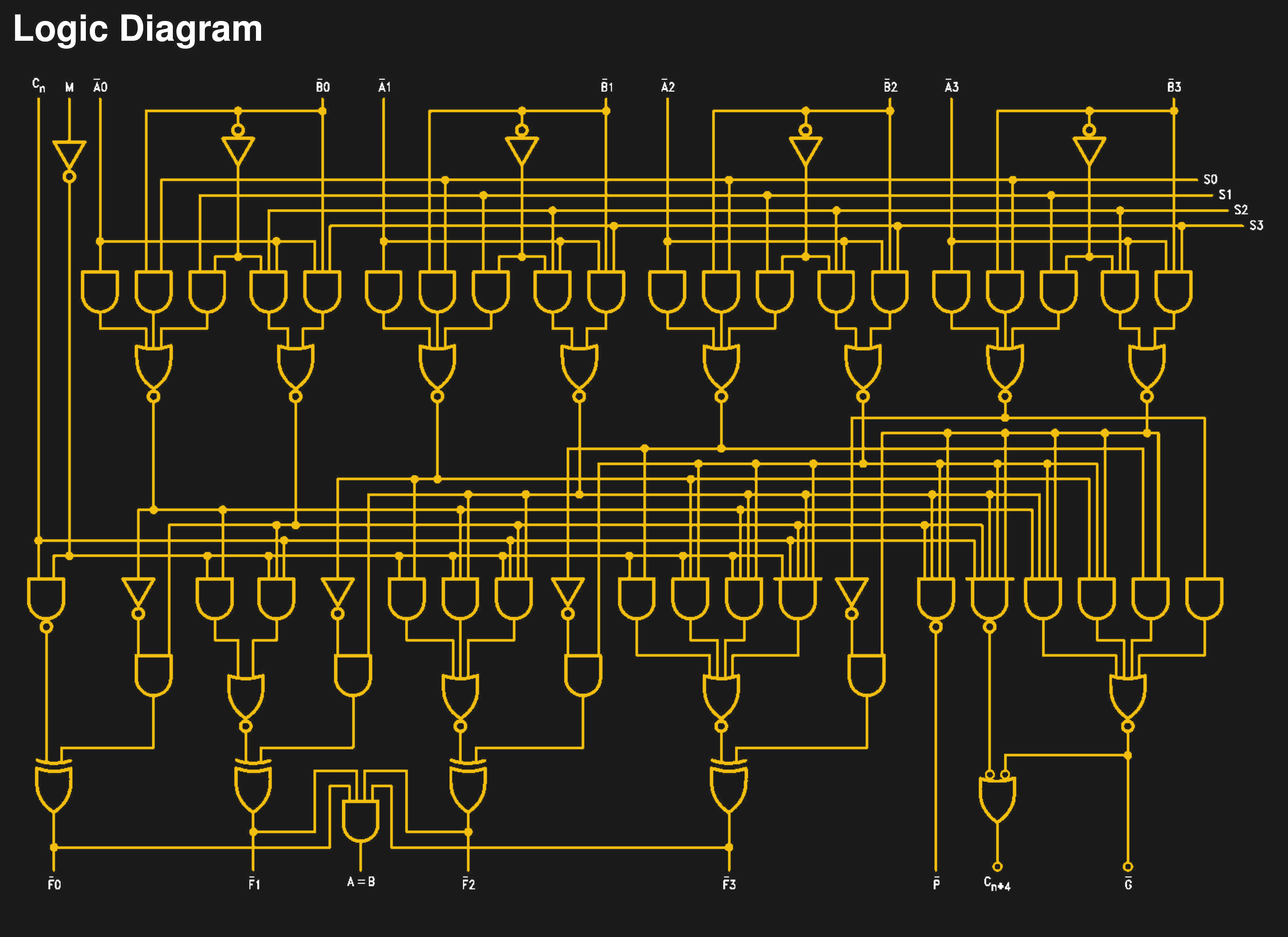
One of the things that every student of digital electronics learns, is that every single logic function can be made from a combination of NAND gates. But nobody is foolhardy enough to give it a try, after all that would require a truly huge number of gates!
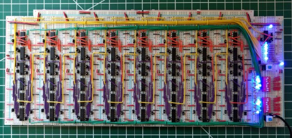
Someone evidently forgot to tell [Notbookies], for he has made a complete 8-bit ALU using only 4011B quad NAND gates on a set of breadboards, and in doing so has created a minor masterpiece with his wiring. It’s inspired by a series of videos from [Ben Eater] describing the construction of a computer with the so-called SAP (Simple As Possible) architecture. The 48 4011B DIP packages sit upon 8 standard breadboards, with an extra one for a set of DIP switches and LEDs, and a set of power busbar breadboards up their sides. He leaves us with the advice borne of bitter experience: “Unless your goal is building a NAND-only computer, pick the best IC for the job“.
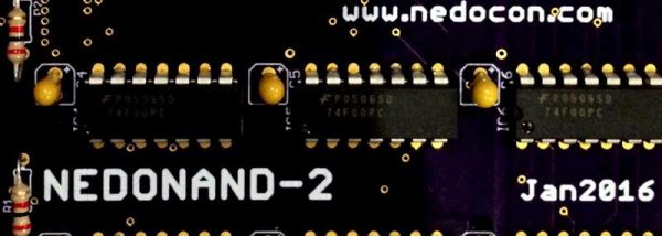
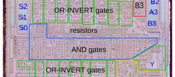
We have covered countless processors and processor components manufactured from discrete logic chips over the years, though this makes them no less impressive a feat. The NedoNAND has been a recent example, a modular PCB-based design. TTL and CMOS logic chips made their debut over 50 years ago so you might expect there to be nothing new from that direction, however we expect this to be well of projects that will keep flowing for may years more.
Via /r/electronics/.
 We have most recently seen [Ken] at work