Al Williams Tells All In The Logic Simulation Hack Chat

The list of requirements for hosting one of our weekly Hack Chats is pretty short: you’ve got to be knowledgeable, passionate, and above all else, willing to put those two quantities on display for a group of like-minded strangers. Beyond that, we’re not too picky. From industry insider to weekend hobbyist, high school dropout to double doctorate, if you’ve got something interesting to talk about, we’re ready to listen.

But in casting a such a wide net, we occasionally forget that we’ve got a considerable collection of potential hosts within our own worldwide roster of contributors. Among this cast of characters, few can boast the same incredible body of knowledge as Al Williams, who was able to pencil in some time this week to host the Logic Simulation Hack Chat.

Or at least, that was the idea. In reality the Chat covered a wide range of topics, and was peppered with fascinating anecdotes pulled from Al’s decades of experience in the field. Though to be fair, we expected no less. He was building hardware before many of us were born, and can take credit for designs that have been at the bottom of the ocean as well as launched into orbit. He’s been writing about it just as long too, with articles of his appearing in iconic print magazines such as Dr. Dobb’s Journal.

Al has seen and done so much that he still surprises us with the occasional nugget, and we’ve been working with him for years. It was only a week or two back that he started a story with “Back when I used to manage a gas pipeline…” in the middle of a conversation about utility metering.

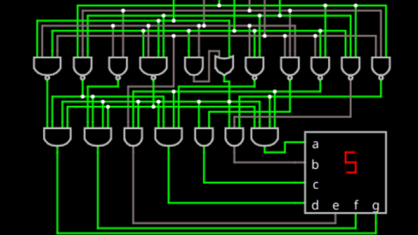
Of course, that’s not to say some technical discussion didn’t sneak in there from time to time. Sure Al’s  recollection of how they used to literally crawl over the schematics for the 68000 back at Motorola might stick out as a particular high point, but he also explains his personal preference for vendor-specific software tools over their more generic open source counterparts. He also draws comparisons between hardware description languages (HDLs) like Verilog and parametric CAD tools such as OpenSCAD in the way that they help model complex relationships in ways that can’t be easily done by more traditional means.

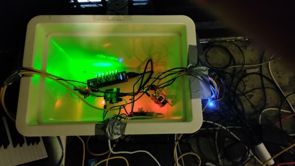
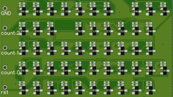
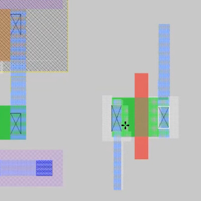
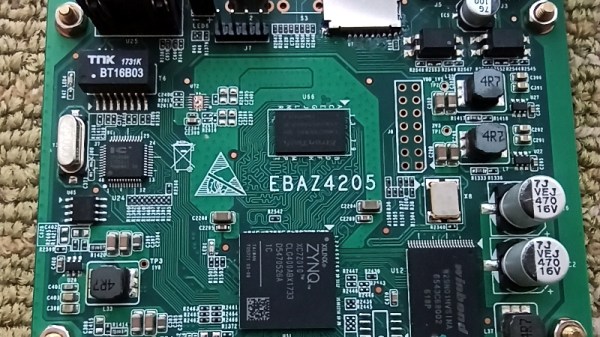
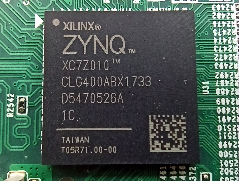
At one point the conversation lingers on the design and production of application-specific integrated circuits (ASICs), and how they compare to field-programmable gate arrays (FPGAs). Traditionally ASICs have been out of reach for the hobbyist, but with the recent collaboration between Google and SkyWater Technology to create an open source process design kit (PDK), they’re now within the capabilities of a dedicated individual. Matt Venn spoke on the topic during Remoticon 2021, and it’s good to see more folks in the community openly discussing the possibilities of custom silicon designed by hackers.

From there, things start really getting wild. From dreaming of virtual reality circuit simulators that let you fly amongst your creations like in Tron, to salivating over high-end technologies such as reflective memory, this Chat really runs the gamut. But then, that’s sort of why we hold them in the first place. Whether you actively participate or are just along for the ride, the Hack Chat gives everyone in the community a chance to gather around a virtual water cooler with fascinating characters that you won’t find anywhere else.


The Hack Chat is a weekly online chat session hosted by leading experts from all corners of the hardware hacking universe. It’s a great way for hackers connect in a fun and informal way, but if you can’t make it live, these overview posts as well as the transcripts posted to Hackaday.io make sure you don’t miss out.

Remoticon 2021 // Matt Venn Helps You Make ASICS

What would you make if you were given about ten square millimeters of space on a silicon wafer on a 130 nm process? That’s the exact question that the Open MPW program asks, and that [Matt Venn] has stepped up to answer. [Matt] came to Remoticon in 2020 to talk about his journey from nothing to his own ASIC, and he came back in 2021 to talk about what has happened in a year.

image of the metal layers of an IC
[maxiborga] has been making beautiful renders of his and others’ chip designs
We expected great designs, but the variety of exciting and wonderful designs that have been submitted we think exceeded our expectations. [Matt] goes through quite a few of them, such as an analog neuron, a RISC-V Arduino-compatible microprocessor, and a satellite transceiver. Perhaps an unexpected side effect has been the artwork. Since the designs are not under an NDA, anyone can take the design and transform it into something gorgeous.

Of course, all of this hardware design isn’t possible without an open toolchain. There is an SRAM generator known as OpenRAM that can generate RAM blocks for your design. Coriolis2 is an RTL to GDS tool that can do placement and routing in VLSI. Finally, FlexCell is a cell library that tries to provide standard functions in a flexible, customizable way that cuts down on the complexity of the layout. There are GitHub actions that can run tests and simulations on PRs to keep the chip’s HDL in a good state.

However, it’s not all roses, and there was an error on the first run (MPW1). Hold time violations were not detected, and the clock tree wasn’t correct. This means that the GPIO cannot be set up, so the designs in the middle could be working, but without the GPIO, it is tricky to determine. With a regular chip, that would be the end, but since [Matt] has access to both the layout and the design, he can identify the problem and come up with a plan. He’s planning on overriding the IO setup shift register with an auxiliary microcontroller. (Ed Note: [tnt] has been making some serious progress lately, summarized in this video.)

It is incredible to see what has come from the project so far, and we’re looking forward to future runs. If this convinces you that you need to get your own ASIC made, you should check out [Matt]’s “Zero to ASIC” course.

Continue reading “Remoticon 2021 // Matt Venn Helps You Make ASICS”

NTP server heated with Bitcoin mining dongles

Bitcoin Mining ASICs Repurposed To Keep NTP Server On Track

They say time is money, but if that’s true, money must also be time. It’s all figurative, of course, but in the case of this NTP server heater powered by Bitcoin mining dongles, money actually does become time.

This is an example of the lengths to which Network Time Protocol aficionados will go in search of slightly better performance from their NTP servers. [Folkert van Heusden], having heard that thermal stability keeps NTP servers happy, used a picnic cooler as an environmental chamber for his  Pi- and GPS-based NTP rig. Heat is added to the chamber thanks to seven Block Erupter ASIC miner dongles, which are turned on by a Python script when a microcontroller sends an MQTT message that the temperature has dropped below the setpoint.

Each dongle produces about 2.5 Watts of heat when it’s working, making them pretty effective heaters. Alas, heat is all they produce at the moment — [Folkert] just has them working on the same hash over and over. He does say that he has plans to let the miners do useful work at some point, not so much for profit but to at least help out the network a bit.

This seems like a bit of a long way around to solve this problem, but since the mining dongles are basically obsolete now — we talked about them way back in 2013 — it has a nice hacky feeling to it that we appreciate.

Using VHDL To Generate Discrete Logic PCB Designs

VHDL and Verilog are hardware description languages, used to describe and define logic circuits. They’re typically used to design ASICs and to program FPGAs, essentially using software to define hardware. However, [Tim] has done something altogether quite creative, creating tools to take VHDL and Verilog and spit out PCB designs for discrete logic. 

Yes, you read that correctly. The basic idea is to take VHDL source code, and then make a PCB layout that implements the desired logic using resistor-transistor logic. From there, the PCB design files can be shipped off to a manufacturer for pick-and-place assembly at a fraction of the cost of producing a bespoke ASIC.

The drawbacks are obvious; tons of individual discrete parts are required, the size penalty is hilariously bad, and power usage is almost certainly orders of magnitude higher than doing the same logic on an ASIC or even FPGA. Oh, and everything’s much slower, too.

However, as an academic exercise or simply for fun, it’s an awesome bit of work. The idea that one can define a complicated logic circuit and have a PCB implementing the logic whipped up by automated tools is amazing, and we absolutely want to see more of this type of thing.

We’ve seen similar work done with VHDL synthesis into 74-series logic design. If you’ve been developing your own fancy digital-logic-fu, be sure to drop us a line!

[Thanks to Yann Guidon for the tip!]

Remoticon Video: From Zero To ASIC; How To Design In Silicon

Designing your own integrated circuits as a one-person operation from your home workshop sounds like science fiction. But 20 years ago, so did rolling your own circuit boards to host a 600 MHz microcontroller with firmware you wrote yourself. Turns out silicon design isn’t nearly as out of reach as it used to be and Matt Venn shows us the ropes in his Zero to ASIC workshop.

Held during the 2020 Hackaday Remoticon, this is a guided tour of the tools used in the Skywater PDK — the Process Design Kit that is an open-source ASIC toolkit produced in a partnership between Google and SkyWater Technology. We covered the news when first announced back in June, but this the most comprehensive look we’ve seen into the actual design process.

Drawing N-channel MOSFET in silicon

Matt builds up the demo starting from the very simple design of an N-channel MOSFET with click-and-drag tools similar to graphics editing software. The good news it that although you can draw your own structures like this, for digital designs you won’t have to. A wide variety of IP has been contributed to the open source project allowing basic building blocks to be pulled in using HDL. However, the power of drawing structures will certainly be the playground for those needing analog design as part of their projects.

As with EDA software used for circuit boards, the PDK includes design rule checks to ensure you aren’t violating the limits of the 130 nm chip fab. There’s some other black magic in there too, as Matt specifically mentions an antenna rules check to safeguard your design from being fried by induced current on “large” (microscopically so) metalized runs during the fabrication process.

Part of a massive logic flow chart for an IC counter design

The current workflow involves grinding through a large number of configuration files, something Matt admits took him a long time to wrap his head around. However, what’s available for proofing your design is very impressing. He demonstrates SPICE simulation to calculate timings, and shows numerous examples of verification drawings generated by the compilation process, either in the form of seeing the structures as they will be laid out, or as logical flow charts. This is crucial as a single run will take 2-3 months to come back from fab — you want to get things right before buttoning up the project. Incidentally, that’s know as “tapeout”, a term you’ve likely heard before and he says it comes from reels of magnetic tape containing the design being removed from the computer and sent to production. Who knew? (This tidbit in strikethrough appears to be incorrect).

But wait, there’s more to this than just designing the things. Part of the intrigue of the Skywater-PDK project is that Google bought into covering a group run about once per quarter so that open-source designs can be ganged onto a multi-project wafer free of charge to the people submitting them. That’s pretty awesome and we’re giddy to hear news of people getting their wafer-level chip scale devices — also known as flip chips — back for testing. Matt is planning a more in-depth paid course on the topic. For now, get a taste of what’s involved from this excellent workshop found after the break.

Continue reading “Remoticon Video: From Zero To ASIC; How To Design In Silicon”

Hacking The FPGA Control Board From A Bitcoin Miner

For anyone serious about mining cryptocurrency such as Bitcoin, we’re well past the point where a standard desktop computer is of much use. While an array of high-end GPUs is still viable for some currencies, the real heavy hitters are using custom mining hardware that makes use of application-specific integrated circuits (ASICs) to crunch the numbers. But eventually even the most powerful mining farm will start to show its age, and many end up selling on the second hand market for pennies on the dollar.

Naturally, hackers are hard at work trying to find alternate uses for these computational powerhouses. While it won’t teach an old ASIC a new trick, [xjtuecho] has documented some very interesting details on the FPGA control board of the Ebit E9+ Bitcoin miner. Known as the EBAZ4205, this board can be purchased for around $20 USD from online importers and even less if you can find one used. Since it’s just the controller it won’t help you build a budget super computer, but there’s always interest in cheap FPGA development boards.

The Zynq SoC combines an FPGA and ARM CPU.

According to [xjtuecho], it takes a little bit of work to get the EBAZ4205 ready for experimentation. For one thing, you may have to solder on your own micro SD slot depending on where you got the board from. You’ll also need to add a couple diodes to configure which storage device to boot from and to select where the board pulls power from.

Once you’re done, you’ll have a dual core Cortex A9 Linux board with 256 MB DDR3 and a Artix-7 FPGA featuring 28K logic elements to play with. Where you go from there is up to you.

This isn’t the first time we’ve seen FPGA boards hit the surplus market at rock bottom prices. When IT departments started dumping their stock of Pano Logic thin clients back in 2013, a whole community of dedicated FPGA hackers sprouted up around it. We’re not sure the if the EBAZ4205 will enjoy the same kind of popularity in its second life, but the price is certainly right.

[Thanks to Rog77 for the tip.]

An Analog IC Design Book Draft

[Jean-Francois Debroux] spent 35 years designing analog ASICs. He’s started a book and while it isn’t finished — indeed he says it may never be — the 180 pages he posted on LinkedIn are a pretty good read.

The 46 sections are well organized, although some are placeholders. There are sections on design flow and the technical aspects of design. Examples range from a square root circuit to a sigma-delta modulator, although some of them are not complete yet. There are also sections on math, physics, common electronics, materials, and tools.

Continue reading “An Analog IC Design Book Draft”