When life hands you a bunch of crummy capacitors, what do you do? Make a whole bunch of temperature sensors, apparently.
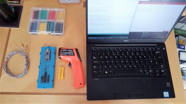
The less-than-stellar caps in question came to [pyromaniac303] by way of one of those all-in-one assortment kits we so love to buy. Stocked with capacitors of many values, kits like these are great to have around, especially when they’ve got high-quality components in them. But not all ceramic caps are created equal, and [pyromaniac303] was determined not to let the lesser-quality units go to waste. A quick look at the data sheets revealed that the caps with the Y5V dielectric had a suitably egregious temperature coefficient to serve as a useful sensor. A fleck of perf-board holds a cap and a series resistor; the capacitor is charged by an Arduino output pin through the resistor, and the time it takes for the input pin connected to the other side of the cap to go high is measured. Charge time is proportional to temperature, and a few calibration runs showed that the response is pretty linear. Unfortunately the temperature coefficient peaks at 10°C and drops sharply below that point, making the sensor useful only on one side of the peak. Still, it’s an interesting way to put otherwise unloved parts to use, and a handy tip to keep in mind.
Temperature sensing isn’t the only trick capacitors can do. We’ve seen them turned into touch sensors before, and used to turn a 3D-printer into a 3D-scanner.