You’d think that the 8086 microprocessor, a 40-year-old chip with a mere 29,000 transistors on board that kicked off the 16-bit PC revolution, would have no more tales left to tell. But as [Ken Shirriff] discovered, reverse engineering the chip from die photos reveals some hidden depths.
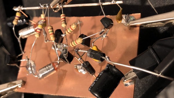
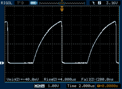
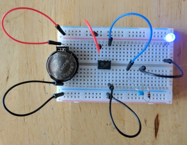
The focus of [Ken]’s exploration of the venerable chip is the charge pump, a circuit that he explains was used to provide a bias voltage across the substrate of the chip. Early chips generally took this -5 volt bias voltage from a pin, which meant designers had to provide a bipolar power supply. To reduce the engineering effort needed to incorporate the 8086 into designs, Intel opted for an on-board charge pump to generate the bias voltage. The circuit consists of a ring oscillator made from a trio of inverters, a pair of transistors, and some diodes to act as check valves. By alternately charging a capacitor and switching its polarity relative to the substrate, the needed -5 volt bias is created.
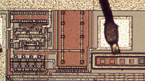
Given the circuit required, it was pretty easy for [Ken] to locate it on the die. The charge pump takes up a relatively huge amount of die space, which speaks to the engineering decisions Intel made when deciding to include it. [Ken] drills down to a very low level on the circuit, with fascinating details on how the MOSFETs were constructed, and why eight transistors were used instead of two diodes. As usual, his die photos are top quality, as are his explanations of what’s going on down inside the silicon.
If you’re somehow just stumbling upon [Ken]’s body of work, you’re in for a real treat. To get you started, you’ll want to check out how he found pi baked into the silicon of the 8087 coprocessor, or perhaps his die-level exploration of different Game Boy audio chips.

