A Peek Under The Hood Of The 741 Op-Amp

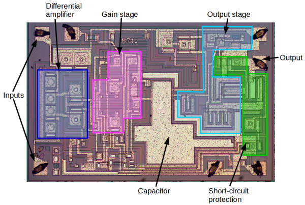
First introduced as an IC back in 1968, but with roots that go back to 1941, the 741 has been tweaked and optimized over the years and is arguably the canonical op-amp. [Ken Shirriff] decided to take a look inside everybody’s favorite op-amp, and ended up with some good-looking photomicrographs and a lot of background on the chip.
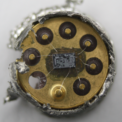
canRather than risk the boiling acid method commonly used to decap epoxy-potted ICs, [Ken] wisely chose a TO-99 can format to attack with a hacksaw. With the die laid bare for his microscope, he was able to locate all the major components and show how each is implemented in silicon. Particularly fascinating is the difference between the construction of NPN and PNP transistors, and the concept of “current mirrors” as constant current sources. And he even whipped up a handy interactive chip viewer – click on something in the die image and find out which component it is on the 741 schematic. Very nice.

We’ve seen lots of chip decappings before, including this reveal of TTL and CMOS logic chips. It’s nice to see the guts of the venerable 741 on display, though, and [Ken]’s tour is both a great primer for the newbie and a solid review for the older hands. Don’t miss the little slice of history he included at the end of the post.

Decapping The CC2630 And CC2650

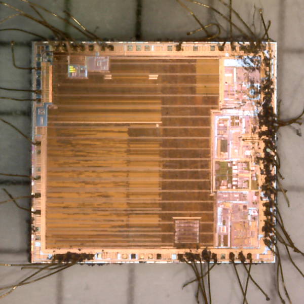
[Jelmer] got curious about the TI CC26XX wireless MCUs and did a little decapping.

TI sells four different models of their CC26XX wireless MCUs. Three support one of the following: RF4CE, Zigbee/6LoWPAN, and Bluetooth and a further model which supports all protocols. Each IC has the same baseline specification: 128Kb Flash, 20Kb RAM and 15 GPIOs. cc26xx_nitric[Jelmer] was curious to know if the price difference was all in the software. And in order to verify this decided that decapping was the only thing to do!

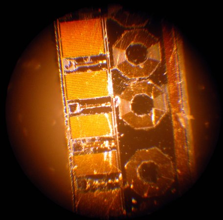
We’ve covered decapping using Nitric acid before, as well as lower tech techniques. Luckily [Jelmer] had access to Nitric acid and a fume hood, not the easiest items to get hold of outside of a research lab (checkout the video of the IC bubbling away below). [Jelmer] got some great die shots under an optical microscope and was able to confirm that the die markings are identical. This opens the door to future hacks, which might allow the cheaper models to be re-flashed, expanding their capabilities.

Continue reading “Decapping The CC2630 And CC2650”

Looking Inside The KR580VM80A Soviet I8080 Clone

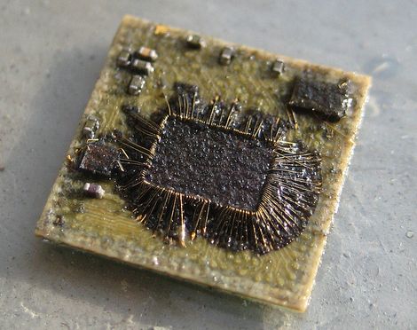
The folks at Zeptobars are on a roll, sometimes looking deep inside historic chips and at others exposing fake devices for our benefit. Behind all of those amazing die shots are hundreds of hours of hard work. [Mikhail] from Zeptobars recently tipped us off on the phenomenal work done by engineer [Vslav] who spent over 1000 hours reverse engineering the Soviet KR580VM80A – one of the most popular micro-controllers of the era and a direct clone of the i8080.

But before [Vslav] could get down to creating the schematic and Verilog model, the chip needed to be de-capped and etched. As they etched down, they created a series of high resolution images of the die. At the end of that process, they were able to determine that the chip had exactly 4758 transistors (contrary to rumors of 6000 or 4500). With the images done, they were able to annotate the various parts of the die, create a Verilog model and the schematic. A tough compatibility test confirmed the veracity of their Verilog model. All of the source data is available via a (CC-BY-3.0) license from their website. If this looks interesting, do check out some of their work that we have featured earlier like comparing real and fake Nordic dies and amazing descriptions of how they figure out the workings of these decapped chips. If this is too deep for you check out the slightly simpler but equally awesome process of delayering PCBs.

Die image of the PCD8544 display controller

Photographing A Display Controller Die

Who doesn’t like integrated circuit porn? After pulling a PCD8544 display controller from an old Nokia phone, [whitequark] disrobed it and took the first public die shot.

As we’ve seen in the past, removing a die from its packaging can be a challenge. It typically involves nasty things like boiling acid. Like many display controllers, the PCD8544 isn’t fully encapsulated in a package. Instead, it is epoxied to a glass substrate.

Removing the glass proved to be difficult. [whitequark] tried a hot plate, a hot air gun, sulphuric acid, and sodium hydroxide with no success. Then the heat was turned up using MAPP gas, which burned the epoxy away.

After some cleaning with isopropanol, the die was ready for its photoshoot. This was done using a standard 30 mm macro lens. Photo processing was done in darktable, an open source photography tool and RAW processor.

[whitequark] plans to take closer photos in the future using more powerful magnification. These high resolution die photos can be useful for a number of things, including finding fake chips and reverse engineering retro hardware.

What’s Inside A USB Isolator?

Coil Die


In this acid powered teardown, [Lindsay] decapped a USB isolator to take a look at how the isolation worked. The decapped part is an Analog Devices ADUM4160. Analog Devices explains that the device uses their iCoupler technology, which consists of on chip transformers.

[Lindsay] followed [Ben Krasnow]’s video tutorial on how to decap chips, but replaced the nitric acid with concentrated sulphuric acid, which is a bit easier to obtain. The process involves heating the chip while applying an acid. Over time, the packaging material is dissolved leaving just the silicon. Sure enough, one of the three dies consisted of five coils that make up the isolation transformers. Each transformer has 15 windings, and the traces are only 4μm thick.

After the break, you can watch a time lapse video of the chip being eaten by hot acid. For further reading, Analog Devices has a paper on how iCoupler works [PDF warning].

[Thanks to Chris for the tip!]

Continue reading “What’s Inside A USB Isolator?”

Reverse Engineering The Die Of A ULN2003 Transistor Array

uln2003-die-reverse-engineering

We’re no strangers to looking at uncapped silicon. This time around it’s not just a show and tell, as one transistor form a ULN2003 chip is reverse engineered.

The photo above is just one slice from a picture of the chip after having its plastic housing remove (decapped). It might be a stretch to call this reverse engineering. It’s more of a tutorial on how to take a functional schematic and figure out how each component is placed on a photograph of a chip die. Datasheets usually include these schematics so that engineers know what to expect from the hardware. But knowing what a resistor or transistor looks like on the die is another story altogether.

The problem is that you can’t just look at a two dimensional image like the one above. These semiconducting elements are manufactured in three dimensions. The article illustrates where the N and P type materials are located on the transistor using a high-res photo and a reference diagram.

If you want to photograph your own chip dies there are a few ways to decap them at home.

Extracting Secured Firmware From Freescale Zigbee Radios

decapped_MC13224

[Travis Goodspeed] recently tore down the Freescale MC13224 wireless radio chip in an effort to demonstrate how the device’s firmware could be read, even when locked down in “secure” mode. While you might not recognize the Freescale MC13224 radio by name alone, you are certainly familiar with some of its practical applications. Found in the QuahogCon and Ninja Party badges among other consumer goods, the popular Zigbee radio turned out to be a fairly easy conquest.

[Travis] first used acid to decap one of the microcontrollers to see what was going on under the plastic casing. Inside, he discovered a discrete flash memory chip, which he removed and repackaged using a wedge wire bonder. He was easily able to extract the firmware, however decapping and repackaging a flash chip isn’t necessarily the most user-friendly process.

After digging further, he discovered that holding one of the chip’s pins low during boot would allow him to run custom code that recovers the firmware image once the pin is pulled high once again. This far more practical means of firmware recovery can be easily facilitated via a circuit board revision, as [Travis] mentions in his blog.