We love a good deep-dive on a specialized piece of technology, the more obscure the better. You’re getting a sneak peek into a world that, by rights, you were never meant to know even existed. A handful of people developed the system, and as far as they knew, nobody would ever come through to analyze and investigate it to find out how it all went together. But they didn’t anticipate the tenacity of a curious hacker with time on their hands.
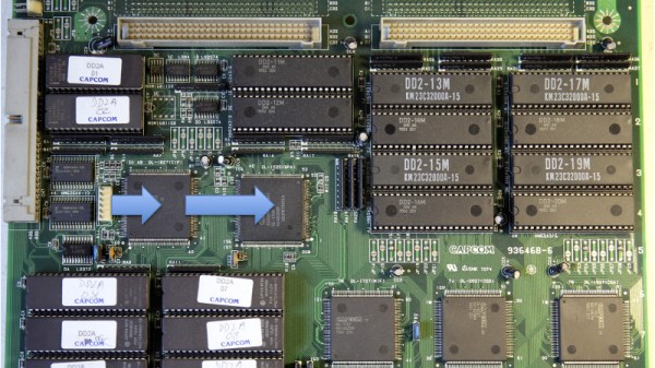
[Eduardo Cruz] has done a phenomenal job of documenting one such system, the anti-piracy mechanisms present in the Capcom CPS2 arcade board. He recently wrote in to tell us he’s posted his third and final entry on the system, this time focusing on figuring out what a mysterious six pin header on the CPS2 board did. Hearing from others that fiddling with this header occasionally caused the CPS2 board to automatically delete the game, he knew it must be something important. Hackaday Protip: If there’s a self-destruct mechanism attached to it, that’s probably the cool part.
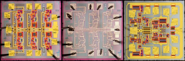
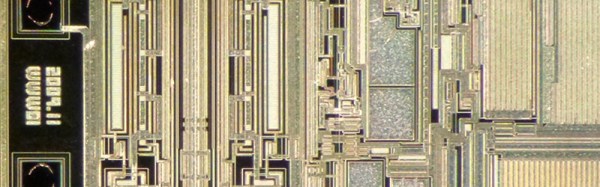
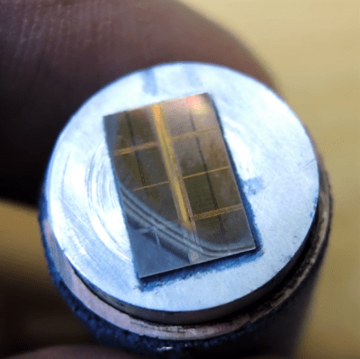
 He followed the traces from the header connector, identified on the silkscreen as C9, back to a custom Capcom IC labeled DL-1827. After decapping the DL-1827 and putting it under the microscope, [Eduardo] made a pretty surprising discovery: it wasn’t actually doing anything with the signals from the header at all. Once the chip is powered up, it simply acts as a pass-through for those signals, which are redirected to another chip: the DL-1525.
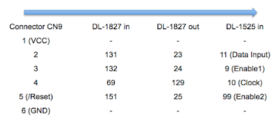
[Eduardo] notes that this deliberate attempt at obfuscating which chips are actually connected to different headers on the board is a classic trick that companies like Capcom would use to try to make it harder to hack into their boards. Once he figured out DL-1525 was what he was really after, he was able to use the information he gleaned from his earlier work to piece together the puzzle.
This particular CPS2 hacking journey only started last March, but [Eduardo] has been investigating the copy protection systems on arcade boards since 2014.
[Thanks to Arduino Enigma for the tip.]
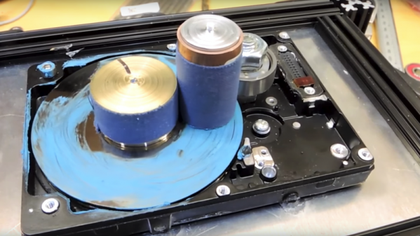
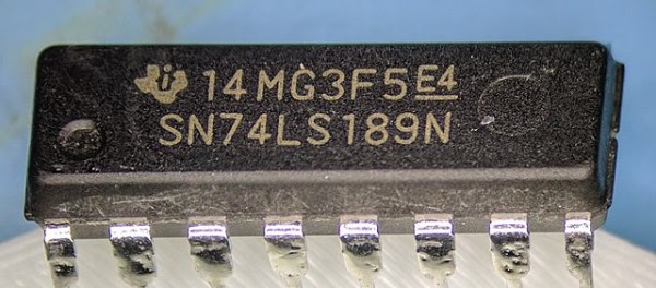
 For those not into the anatomy and physiology of semiconductors, getting a look at the inside of the chip can reveal valuable information needed to reverse engineer a device, or it can just scratch the itch of curiosity. Lapping (the gentle grinding away of material) is one way to see the layers that make up the silicon die that lies beneath the epoxy. Hard drives designed to spin at 7200 rpm or more hardly seem a suitable spinning surface for a gentle lapping, but [electronupdate] just wanted the platter for its ultra-smooth, ultra-flat surface.