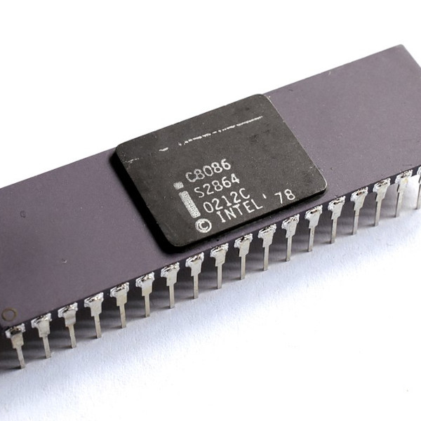
Various hardware components laid out on a workbench.

Working On Open-Source High-Speed Ethernet Switch

Our hacker [Andrew Zonenberg] reports in on his open-source high-speed Ethernet switch. He hasn’t finished yet, but progress has been made.

If you were wondering what might be involved in a high-speed Ethernet switch implementation look no further. He’s been working on this project, on and off, since 2012. His design now includes a dizzying array of parts. [Andrew] managed to snag some XCKU5P FPGAs for cheap, paying two cents in the dollar, and having access to this fairly high-powered hardware affected the project’s direction.

Continue reading “Working On Open-Source High-Speed Ethernet Switch”

MiSTER Multisystem 2 on a wooden table

MiSTer For Mortals: Meet The Multisystem 2

If you’ve ever squinted at a DE10-Nano wondering where the fun part begins, you’re not alone. This review of the Mr. MultiSystem 2 by [Lee] lifts the veil on a surprisingly noob-friendly FPGA console that finally gets the MiSTer experience out of the tinker cave and into the living room. Developed by Heber, the same UK wizards behind the original MultiSystem, this follow-up console dares to blend flexibility with simplicity. No stack required.

It comes in two varieties, to be precise: with, or without analog ports. The analog edition features a 10-layer PCB with both HDMI and native RGB out, Meanwell PSU support, internal USB headers, and even space for an OLED or NFC reader. The latter can be used to “load” physical cards cartridge-style, which is just ridiculously charming. Even the 3D-printed enclosure is open-source and customisable – drill it, print it, or just colour it neon green. And for once, you don’t need to be a soldering wizard to use the thing. The FPGA is integrated in the mainboard. No RAM modules, no USB hub spaghetti. Just add some ROMs (legally, of course), and you’re off.

Despite its plug-and-play aspirations, there are some quirks – for example, the usual display inconsistencies and that eternal jungle of controller mappings. But hey, if that’s the price for versatility, it’s one you’d gladly pay. And if you ever get stuck, the MiSTer crowd will eat your question and spit out 12 solutions. It remains 100% compatible with the MiSTer software, but allows some additional future features, should developers wish to support them.

Want to learn more? This could be your entrance to the MiSTer scene without having to first earn a master’s in embedded systems. Will this become an alternative to the Taki Udon announced Playstation inspired all-in-one FPGA console? Check the video here and let us know in the comments. Continue reading “MiSTer For Mortals: Meet The Multisystem 2”

Fancy Adding A Transputer Or Two To Your Atari ST?

Has anybody heard of the ATW800 transputer workstation? The one that used a modified Atari ST motherboard as a glorified I/O controller for a T-series transputer?  No, we hadn’t either, but transputer superfan [Axel Muhr] has created the ATW800/2, an Atari Transputer card, the way it was meant to be.

The transputer was a neat idea when it was conceived in the 1980s. It was designed specifically for parallel and scientific computing and featured an innovative architecture and dedicated high-speed serial chip-to-chip networking. However, the development of more modern buses and general-purpose CPUs quickly made it a footnote in history. During the same period, a neat transputer-based parallel processing computer was created, which leveraged the Atari ST purely for its I/O. This was the curious ATW800 transputer workstation. That flopped as well, but [Axel] was enough of a fan to take that concept and run with it. This time, rather than using the Atari as a dumb I/O controller, the card is explicitly designed for the Mega-ST expansion bus. A second variant of the ATW800/2 is designed for the Atari VME bus used by the STe and TT models—yes, VME on an Atari—it was a thing.

Continue reading “Fancy Adding A Transputer Or Two To Your Atari ST?”

Homemade VNA Delivers High-Frequency Performance On A Budget

With vector network analyzers, the commercial offerings seem to come in two flavors: relatively inexpensive but limited capabilities, and full-featured but scary expensive. There doesn’t seem to be much middle ground, especially if you want something that performs well in the microwave bands.

Unless, of course, you build your own vector network analyzer (VNA). That’s what [Henrik Forsten] did, and we’ve got to say we’re even more impressed by the results than we were with his earlier effort. That version was not without its problems, and fixing them was very much on the list of goals for this build. Keeping the build affordable was also key, which resulted in some design compromises while still meeting [Henrik]’s measurement requirements.

The Bill of Materials includes dual-channel broadband RF mixer chips, high-speed 12-bit ADCs, and a fast FPGA to handle the torrent of data and run the digital signal processing functions. The custom six-layer PCB is on the large side and includes large cutouts for the directional couplers, which use short lengths of stripped coaxial cable lined with ferrite rings. To properly isolate signals between stages, [Henrik] sandwiched the PCB between a two-piece aluminum enclosure. Wisely, he printed a prototype enclosure and lined it with aluminum foil to test for fit and function before committing to milling the final version. He did note some leakage around the SMA connectors, but a few RF gaskets made from scraps of foil and solder braid did the trick.

This is a pretty slick build, especially considering he managed to keep the price tag at a very reasonable $300. It’s more expensive than the popular NanoVNA or its clones, but it seems like quite a bargain considering its capabilities.

A slide from a talk about Spade language with a diagram about how it fits in with Verilog, VHDL, and HLS.

The Spade Hardware Description Language

Spade is an open-source hardware description language (HDL) developed at Linköping University, Sweden.

Other HDLs you might have heard of include Verilog and VHDL. Hardware engineers use HDLs to define hardware which can be rendered in silicon. Hardware defined in HDLs might look like software, but actually it’s not software, it’s hardware description. This hardware can be realized myriad ways including in an FPGA or with an ASIC.

You have probably heard that your CPU processes instructions in a pipeline. Spade has first-class support for such pipelines. This means that design activities such as re-timing and re-pipelining are much easier than in other HDLs where the designer has to implement these by hand. (Note: backward justification is NP-hard, we’re not sure how Spade supports this, if it does at all. If you know please enlighten us in the comments!)

Spade implements a type system for strong and static typing inspired by the Rust programming language and can do type inference. It supports pattern matching such as you might see in a typical functional programming language. It boasts having user-friendly and helpful error messages and tooling.

Spade is a work in progress so please expect missing features and breaking changes. The documentation is in The Spade Book. If you’re interested you can follow development on GitLab or Discord.

So now that you know about the Spade language, are you planning to take it for a spin? You will find plenty of Verilog/VHDL designs at Hackaday which you could re-implement using Spade, such as an easy one like Breathing LED Done With Raw Logic Synthesized From A Verilog Design (see benchmarks) or a much more challenging one like Game Boy Recreated In Verilog. If you give Spade a go we’d love to see what you come up with!

Continue reading “The Spade Hardware Description Language”

Reconfigurable FPGA For Single Photon Measurements

Detecting single photons can be seen as the backbone of cutting-edge applications like LiDAR, medical imaging, and secure optical communication. Miss one, and critical information could be lost forever. That’s where FPGA-based instrumentation comes in, delivering picosecond-level precision with zero dead time. If you are intrigued, consider sitting in on the 1-hour webinar that [Dr. Jason Ball], engineer at Liquid Instruments, will host on April 15th. You can read the announcement here.

Before you sign up and move on, we’ll peek into a bit of the matter upfront. The power lies in the hardware’s flexibility and speed. It has the ability to timestamp every photon event with a staggering 10 ps resolution. That’s comparable to measuring the time it takes light to travel just a few millimeters. Unlike traditional photon counters that choke on high event rates, this FPGA-based setup is reconfigurable, tracking up to four events in parallel without missing a beat. From Hanbury-Brown-Twiss experiments to decoding pulse-position modulated (PPM) data, it’s an all-in-one toolkit for photon wranglers. [Jason] will go deeper into the subject and do a few live experiments.

Measuring single photons can be achieved with photomultipliers as well. If exploring the possibilities of FPGA’s is more your thing, consider reading this article.

Game Bub Plays ROMs And Cartridges

With today’s technology, emulating video game consoles from the 90s or before is trivial. A Raspberry Pi and a controller of some sort is perhaps the easiest and simplest way to go to get this job done, but to really impress the masses some extra effort is required. This handheld from [Eli] called the Game Bub not only nails the appearance and feel of the first three generations of Nintendo handhelds but, thanks to its FPGA, can play not only ROMs but the original game cartridges as well.

As [Eli] notes, the FPGA is not strictly necessary for emulation, but does seem to be better at interfacing with physical hardware like controllers and game cartridges. For this task an Xilinx XC7A100T with integrated memory was chosen, with a custom PCB supporting the built-in controller, speaker, a rechargeable lithium battery, and a 480×320 display (that had to be rotated out of portrait mode). An SD Card reader is included for any ROM files, and there’s also a ESP32-S3 included to give the handheld WiFi and Bluetooth capabilities, with future plans to support the communications protocol used by the Game Boy Advance Wireless Adapter.

There are a few other features with the Game Bub as well, including the ability to use an authentic link cable to communicate with the original Game Boy and Game Boy Color, and a Switch-like dock that allows the Game Bub to be connected to an external monitor. It’s also open source, which makes it an even more impressive build. Presumably it doesn’t include the native ability to dump cartridges to ROM files but you don’t need much more than a link cable to do that if you need to build your ROM library.

Continue reading “Game Bub Plays ROMs And Cartridges”