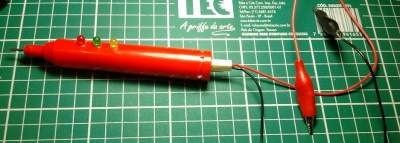
[Robert Morrison] had an ancient HP 545A logic probe, which was great for debugging SMT projects. The only problem was that being 45 years old, it wasn’t quite up to scratch when it came to debugging today’s faster circuitry. Thus, he hacked it to do better, and entered it in our 2025 One Hertz Challenge to boot!
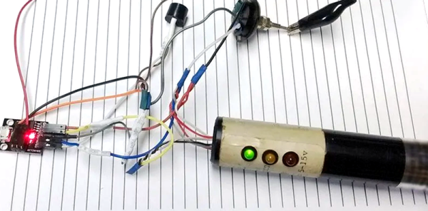
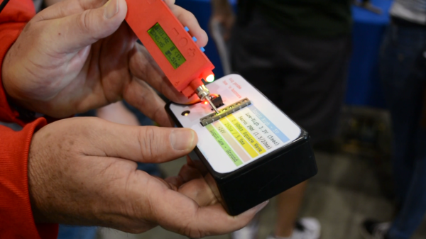
[Robert’s] hack relied on the classic logic probe for its stout build and form factor, which is still useful even on today’s smaller hardware. Where it was lacking was in dealing with circuits running at 100 MHz and above. To rectify this, [Robert] gave the probe a brain transplant with a Sparkfun Alorium FPGA board and a small display. The FPGA is programmed to count pulses while measuring pulse widths and time, and it then drives the display to show this data to the user. There’s also a UART output, and [Robert] is actively developing further logic analyzer features, too.
You might be questioning how this project fits in the One Hertz Challenge, given it’s specifically built for running at quite high speeds. [Robert] snuck it in under the line because it resamples and updates the display on a once-a-second basis. Remember, as per the challenge site—”For this challenge, we want you to design a device where something happens once per second.” We’re giving you a lot of leeway here!
Often, old scopes and probes and other gear are really well built. Sometimes, it’s worth taking the best of the old physical hardware and combining it with modern upgrades to make something stout that’s still useful today. Meanwhile, if you’re cooking up your own neo-retro-logic probes, don’t hesitate to notify the tipsline!


