Oscilloscope And Microscope Augmented With Ghosts

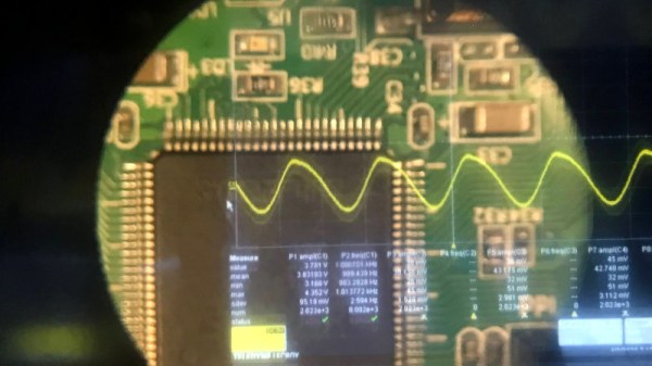
Augmented reality saw a huge boom a few years ago, where an image of the real world has some virtual element layer displayed on top of it. To get this effect to work, however, you don’t need a suite of software and smart devices. [elad] was able to augment a microscope with the output from an oscilloscope, allowing him to see waveforms while working on small printed circuit boards with the microscope.

The build relies on a simplified version of the Pepper’s Ghost illusion. This works by separating two images with a semi-transparent material such as glass, placed at an angle. When looking through the material, the two images appear to blend together. [elad] was able to build a box that attaches to the microscope with a projection of the oscilloscope image augmented on the view of the microscope.

This looks like it would be incredibly useful for PCBs, especially when dealing with small SMD components. The project is split across two entries, the second of which is here. In one demonstration the oscilloscope image is replaced with a visual of a computer monitor, so it could be used for a lot more applications than just the oscilloscope, too. There aren’t a lot of details on the project page though, but with an understanding of Pepper’s Ghost this should be easily repeatable. If you need more examples, there are plenty of other builds that use this technique.

Continue reading “Oscilloscope And Microscope Augmented With Ghosts”

Making PCBs With A Vinyl Cutter

You might assume that you need a lot of expensive stuff to make your own PCBs, but that isn’t the case: you can do it with a vinyl cutter and a few common chemicals and tools. [Emiliano Valencia] has laid out the entire process. While we’ve seen plenty of make your own PCB guides before, this one goes a bit further as it covers using the vinyl cutter to make solder masks, so you can use it for surface mount designs.

The end result of the process that [Emilano] lays out is the tinyDice, a cute little electronic die that can fit on a keyring. The whole process is very well written up, and even experienced PCB makers will probably find a few useful tricks here.

The really interesting part for us was using the vinyl cutter to make three parts of the process: the etching mask, the solder mask that protects the traces and the solder stencil that applies the solder to the pads for surface mounting. Continue reading “Making PCBs With A Vinyl Cutter”

Thermochromic Display Tells You The Temperature Despite Your Current Mood

Readers who survived the 1970s will no doubt remember the “mood ring” fad, where a liquid crystal mounted to a ring would magically reveal your current emotional state to all and sundry by changing color. This nifty thermochromic display is based on the same principle, and while it might not start a new craze, it’s still pretty mesmerizing to watch.

This isn’t [Moritz v. Sivers]’ first attempt at a thermochromic display. His earlier version was far more complicated, using separate copper plates clad with thermochromic film for each segment, with Peltier devices to cool and heat them individually. Version two is much simpler, using a printed circuit board with heating elements in the shape of seven-segment displays etched into it. The thermochromic film sits directly on the heater PCB; a control PCB below has the MCU and sensors on it. The display alternates between temperature and humidity, with the segments fading in an uneven and ghostly way that really makes this fun to watch. [Moritz] has made the build files available, and there’s a detailed Instructable as well.

We’re always on the lookout for alternate display modalities, especially when they look this cool. We’ve seen other thermochromic displays before, of course, and persistence of phosphorescence looks great, too.

Continue reading “Thermochromic Display Tells You The Temperature Despite Your Current Mood”

PCB Finishes Hack Chat

Join us on Wednesday, March 11 at noon Pacific for the PCB Finishes Hack Chat with Mark Hughes and Elijah Gracia!

There’s no way to overestimate the degree to which the invention of the printed circuit board revolutionized electronics. What was once the work of craftspeople weaving circuits together with discrete components, terminal strips, and wiring harnesses could now be accomplished with dedicated machines, making circuit construction an almost human-free process. And it was all made possible by figuring out how to make copper foil stick to a flat board, and how to remove some of it while leaving the rest behind.

​Once those traces are formed, however, there’s more work to be done. Bare copper is famously reactive stuff, and oxides soon form that will make the traces difficult to solder later. There are hundreds of different ways to prevent this, and PCB surface finishing has become almost an art form itself. Depending on the requirements for the circuit, traces can be coated with tin, lead, gold, nickel, or any combination of the above, using processes ranging from electroplating to immersion in chemical baths. And the traces aren’t the only finishes; solder resist and silkscreening are both important to the usability and durability of the finished board.

For this Hack Chat, we’ll be talking to Elijah Gracia and Mark Hughes from Royal Circuit Solutions. They’re both intimately familiar with the full range of PCB coatings and treatments, and they’ll help us make sense of the alphabet soup​: HASL, OSP, ENIG, IAg, LPI, and the rest. We’ll learn what the different finishes do, which to choose under what circumstances, and perhaps even learn a bit about how to make our homebrew boards look a little more professional and perform a bit better.

join-hack-chatOur Hack Chats are live community events in the Hackaday.io Hack Chat group messaging. This week we’ll be sitting down on Wednesday, March 11 at 12:00 PM Pacific time. If time zones have got you down, we have a handy time zone converter.

Click that speech bubble to the right, and you’ll be taken directly to the Hack Chat group on Hackaday.io. You don’t have to wait until Wednesday; join whenever you want and you can see what the community is talking about.

3D Printing For Wire Paths Yields An Arduboy Minus The PCB

What is part way between a printed circuit board and a rats-nest of point-to-point wiring? We’re not sure, but this is it. [Johan von Konow] has come up with an inspired solution, 3D printing an Arduboy case with channels ready-made for all the wires. The effect with his 3DPCBoy is of a PCB without the PCB, and allows the console to be made very quickly and cheaply.

The Arduboy — which we originally looked at back in 2014 — is a handheld gaming console in a somewhat Gameboy-like form factor. Normally a credit-card sized PCB hosts all the components, including a microcontroller, display, and buttons. Each has a predictable footprint and placement so they can simply be wired together with hookup wire, if you don’t mind a messy result.

Here the print itself has all the holes ready-created for the components, and the path of the wires has a resemblance to the sweeping traces of older hand-laid PCBs. The result is very effective way to take common components — and Arduino pro micro board for the uC, an OLED breakout board, and some buttons — and combine them into a robust package. This technique of using 3D prints as a combination of enclosure and substrate for components and wiring has an application far beyond handheld gaming. We look forward to seeing more like it.

[Via the Arduboy community forum, thanks Kevin Bates for the tip.]

Debugging PCBs With Augmented Reality

Mihir Shah has designed many a PCB in his time. However, when working through the development process, he grew tired of the messy, antiquated methods of communicating design data with his team. Annotating photos is slow and cumbersome, while sending board design files requires everyone to use the same software and be up to speed. Mihir thinks he has a much better solution by the name of InspectAR, it’s an augmented reality platform that lets you see inside the circuit board and beyond which he demoed during the 2019 Hackaday Superconference.

The InspectAR package makes it easy to visualise signals on the board.

The idea of InspectAR is to use augmented reality to help work with and debug electronics. It’s a powerful suite of tools that enable the live overlay of graphics on a video feed of a circuit board, enabling the user to quickly and effectively trace signals, identify components, and get an idea of what’s what. Usable with a smartphone or a webcam, the aim is to improve collaboration and communication between engineers by giving everyone a tool that can easily show them what’s going on, without requiring everyone involved to run a fully-fledged and expensive electronics design package.

The Supercon talk served to demonstrate some of the capabilities of InspectAR with an Arduino Uno. With a few clicks, different pins and signals can be highlighted on the board as Mihir twirls it between his fingers. Using ground as an example, Mihir first highlights the entire signal. This looks a little messy, with the large ground plane making it difficult to see exactly what’s going on. Using an example of needing a point to attach to for an oscilloscope probe, [Mihir] instead switches to pad-only mode, clearly revealing places where the user can find the signal on bare pads on the PCB. This kind of attention to detail shows the strong usability ethos behind the development of InspectAR, and we can already imagine finding it invaluable when working with unfamiliar boards. There’s also the possibility to highlight different components and display metadata — which should make finding assembly errors a cinch. It could also be useful for quickly bringing up datasheets on relevant chips where necessary.

Obviously, the electronic design space is a fragmented one, with plenty of competing software in the market. Whether you’re an Eagle diehard, Altium fanatic, or a KiCad fan, it’s possible to get things working with InspectAR. Mihir and the team are currently operating out of office space courtesy of Autodesk, who saw the value in the project and have supported its early steps. The software is available free for users to try, with several popular boards available to test. As a party piece for Supercon, our very own Hackaday badge is available if you’d like to give it a spin, along with several Arduino boards, too. We can’t wait to see what comes next, and fully expect to end up using InspectAR ourselves when hacking away at a fresh run of boards!

Review: Testdriving LibrePCB Shows That It’s Growing Up Fast

There are a host of PCB CAD tools at the disposal of the electronic designer from entry-level to multi-thousand-dollar workstation software. It’s a field in which most of the players are commercial, and for the open-source devotee there have traditionally been only two choices. Both KiCad and gEDA are venerable packages with legions of devoted fans, but it is fair to say that they both present a steep learning curve for newcomers. There is however another contender in the world of open-source PCB CAD, in the form of the up-and-coming LibrePCB.

This GPL-licensed package has only been in development for a few years. LibrePCB brought out its first official release a little over a year ago, and now stands at version 0.1.3 with builds for GNU/Linux, Windows, MacOS, and FreeBSD. It’s time to download it and run it through its paces, to see whether it’s ready to serve its purpose.

Continue reading “Review: Testdriving LibrePCB Shows That It’s Growing Up Fast”