Letting [Euler] Help Out With PCB Fabrication

drillin

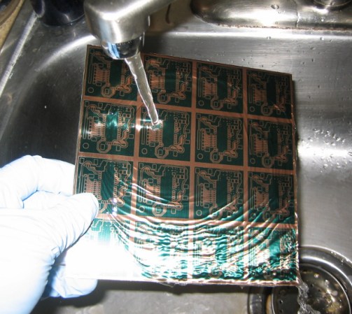
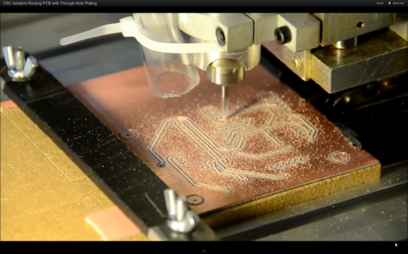
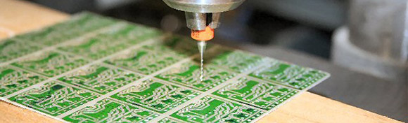
Since [Alessio] has been etching his own PCBs, he’s hit upon the most tedious part of the process, and the reason homebrew SMD boards are so awesome: drilling your own boards is a pain. While [Alessio]’s CNC mill takes care of most of the work, aligning the pre-drilled boards and correcting for any scaling issues from the mask is a bit difficult. With the help of a transform matrix, though, drilling PCBs has never been easier.

While the Gcode running the mill may be accurate, the actual manufactured PCBs might not be. If the extents on [Alessio]’s board aren’t exactly aligned with the axes of the CNC mill, the drill holes end up where they’re supposed to be. To solve this problem, [Alessio] wrote a PCB drilling transformational matrix calculator. The basic idea is by drilling just a few holes, [Alessio] is able to calculate any offset required in the Gcode with the help of a little bit of linear algebra.

Toner Transfer For Resist And Silk Screen Using Printable Vinyl

This toner transfer method uses a different material than we normally see. The red sheet being peeled back isn’t toner transfer paper. It’s printable vinyl used for both the resist and the silk screen.

The application process is almost the same as any other toner transfer PCB fabrication material. The printable vinyl stick is first adhered to a piece of paper before feeding it through a laser printer. It is acceptable to clean the vinyl with alcohol before printing if you think there may be a finger print or other oil on its surface. After printing it is carefully aligned with the board and ironed on.

[Mincior Vicentiu] thinks there are a few big benefits to this material. It seems that as you heat the toner it expands and hardens, but the vinyl actually softens to make room for this. We can imagine that this helps alleviate the smudging that sometimes occurs when ironing toner that is simply printed on paper. The other advantage is that the vinyl peels off quite easily after ironing, where as you need to soak paper in water and carefully massage it off of the toner.

[via Dangerous Prototypes]

Comprehensive Home PCB Fabrication Tutorial

home-pcb-fabrication

From what we’ve seen we’d say [Jianyi Liu] is really good at etching PCBs at home. Now you can learn from his experience. He just published a mammoth guide to fabricating your own PCBs at home. That link goes to his index page which leads to all eight parts of the guide.

He starts off by mentioning that fab house boards are rather inexpensive these days. This will save you a lot of trouble (like acquiring the equipment and raw materials needed to get up and running) but you can’t beat the turnaround time of doing it yourself.

After discussing the particulars about trace width, copper thickness, and a few design considerations he lays out his board and prints the artwork to a sheet of transparency film. A pre-sensitized board is cut to size before a trip through an exposure rig with the film taped onto it. The image above shows him rinsing the board after applying the developer chemical. From here he uses cupric chloride he mixed himself to etch the board. [Jianyi] recommends populating the components before cutting the panel apart — a task which he accomplishes with a hack saw.

Automated PCB Panelization

panel

Some PCB production houses – Seeed Studio and itead studio, especially – allow you to upload a gerber file and receive a printed circuit board very inexpensively. The pricing structure for these board houses is based on predesignated board sizes – 5cm square or 5×10 cm – and sometimes a project is just too small to justify buying a full 25 square centimeters of board. This is where panelizing comes in: by putting multiple copies of a circuit board on one of the available sizes you can get more boards for the same amount of money. But how to panelize your boards without the (sometimes) hassle of cutting and pasting?

[Martin] came up with a way of panelizing PCBs with just a Python script. By creating one copy of a circuit board in KiCAD, he can fire up his script and tell the computer exactly how to duplicate his circuit to fit any size board.

By his own admission, [Martin]’s script is still a little clunky, but it does allow him to edit the panelized board in KiCAD and also copies the nets so the ratsnest doesn’t go between boards.

Level Converters To Make All Your Hardware (5.5V And Under) Play With Each Other

txb0108-level-converters-ks0108-stellaris-launchpad

I finally set aside some time for one of my own projects. I have been playing around with ARM microcontrollers a lot lately and wanted to try out my GLCD display that uses the KS0108 protocol. It’s 5V but I had heard that some of these displays will work with 3.3V TTL. But the datasheet tells me otherwise. I tried using a pull-up resistor to 5V and configuring the Stellaris Launchpad pins to open drain, but the low voltage wasn’t getting below the 0.3V threshold needed by my display. My only choice was to use some type of level conversion. I actually ended up driving the KS0108 using a pair of TXB0108 level converters.

I figured this had to have been done before so I check over at Sparkfun. Their offerings are either one-way or have a direction pin that you must drive yourself. I figured there had to be a bi-directional solution and a search over at Mouser led me to the TXB0108. It is exactly what I was looking for and as you can see I etched my own circuit boards to make the TSSOP chips breadboard compatible. I’ve documented the process you can find the code and board files at my post linked above.

Update: one of the Reddit comments mentions this chip is available on a breakout board from Adafruit if you’re interested.

Through Hole Plating And Milling At Home

Here’s a PCB fabrication process that makes us envious. It’s pretty darn close to fab-house quality at home. [Cpirius] is using a CNC mill and through hole plating technique to produce his double-sided circuit boards.

The video embedded after the break shows one board from start to finish. It begins with the mill drilling holes through some double-sided copper clad stock. Once the millings have been cleaned off the holes are coated with a mixture of waterproof ink and carbon. This prepares them for plating by making the holes themselves conductive. The board is then run through an electroplating process based on this guide.

Possibly the most interesting part of the process starts 52 seconds into the clip. The mill uses a conductive probe to generate a height map of the entire board. This allows it to vary the routing depth for perfectly cut isolation traces. That final routing process is pictured above.

Continue reading “Through Hole Plating And Milling At Home”

MSP430 Launchpad Game Of Life Shield

[100uf] built an LED matrix shield for the MSP430 launchpad. His goal with this design was to have it play Conway’s Game of Life. It does just that, as you can see in the clip after the break. But it’s just waiting to learn some more tricks. After he tires of watching the cellular automaton he can try his hand at making some LED pendant animations.

As you can tell, the board was made in his home workshop. It’s not etched, but milled using the CNC machine shown in this image gallery. This is a single-sided PCB, which works well enough for the surface mount components and the downward facing pin sockets. But we wonder how difficult it was to solder the legs of that 8×8 LED matrix. It does have plastic feet at each corner that serve as standoffs to separate the body from the copper layer. But it still looks like a tight space into which he needed to get his iron and some solder.

Continue reading “MSP430 Launchpad Game Of Life Shield”