What’s Coming In KiCad Version 5

Way back in the day, at least five years ago, if you wanted to design a printed circuit board your best option was Eagle. Now, Eagle is an Autodesk property, the licensing model has changed (although there’s still a free version, people) and the Open Source EDA suite KiCad is getting better and better. New developers are contributing to the project, and by some measures, KiCad is now the most popular tool to develop Open Source hardware.

At FOSDEM last week, [Wayne Stambaugh], project lead of KiCad laid out what features are due in the upcoming release of version 5. KiCad just keeps improving, and these new features are really killer features that will make everyone (unjustly) annoyed with Eagle’s new licensing very happy.

Although recent versions of KiCad have made improvements to the way part and footprint libraries are handled, the big upcoming change is that footprint libraries will be installed locally. The Github plugin for library management — a good idea in theory — is no longer the default. Spice simulation is also coming to KiCad. The best demo of the upcoming Spice integration is this relatively old video demonstrating how KiCad turns a schematic into graphs of voltage and current.

The biggest news, however, is the new ability to import Eagle projects. [Wayne] demoed this live on stage, importing an Eagle board and schematic of an Arduino Mega and turning it into a KiCad board and schematic in a matter of seconds. It’s not quite perfect yet, but it’s close and very, very good.

There are, of course, other fancy features that make designing schematics and PCBs easier. Eeschema is getting a better configuration dialog, improved bus and wire dragging, and improved junction handling. Pcbnew is getting rounded rectangle and complex pad shape support, direct export to STEP files, and you’ll soon be able to update the board from the schematic without updating the netlist file. Read that last feature again, slowly. It’s the best news we’ve ever heard.

Additionally, this is one of the rare times you get to hear [Wayne] speak. This means the argument over the pronunciation of KiCad is over. It’s ‘Key-CAD‘ not ‘Kai-CAD‘. You can check out the entirety of [Wayne]’s State of the KiCad talk below.

Continue reading “What’s Coming In KiCad Version 5”

Making An Arduino Shield PCB With Fritzing

[Allan Schwartz] decided to document his experience using Fritzing to design, fabricate, and test a custom Arduino shield PCB, and his step-by-step documentation makes the workflow very clear. Anyone who is curious or has been looking for an opportunity to get started will find [Allan]’s process useful to follow. The PCB in question has two shift registers, eight LEDs, eight buttons, and fits onto an Arduino; it’s just complex enough to demonstrate useful design features and methods while remaining accessible.

[Allan] starts with a basic breadboard design, draws a schematic, prototypes the circuit, then designs the PCB and orders it online, followed by assembly and testing. [Allan] had previously taught himself to use Eagle and etched his own PCBs via the toner transfer method, but decided to use Fritzing instead this time around and found it helpful and easy to use.

About a year ago we saw Fritzing put through its paces for PCB design, and at the time found that it didn’t impress much from an engineering perspective. Regardless, as a hobbyist [Allan] found real value in using Fritzing for his project from beginning to end; he documented both the process and his observations in order to help others, and that’s wonderful.

A Tool For KiCad Board Renderings

If you’re producing documentation for a PCB project, you might as well make the board renders look good. But then, that’s a lot of work and you’re not an artist. Enter [Jan]’s new tool that takes KiCad board files, replaces each footprint with (custom) graphics, and provides a nice SVG representation, ready for labelling. If you like the output of a Fritzing layout, but have higher expectations of the PCB tool, this is just the ticket.

We all love [pighixx]’s pinout diagrams. Here’s his take on the Arduino Uno, for instance. It turns out that he does these largely by hand. That’s art for ya.

Sparkfun has taken a stab at replicating the graphical style for the pin labels, but then they toss in a photo of the real item. [Jan]’s graphic PCB generator fills in the last step toward almost putting [pighixx] out of a job. Get the code for yourself on GitHub.

Design And Hacking Drilldown: SuperCon Badge

One can imagine a political or business conference without an interactive badge — but not a hacker conference. Does this make the case for hackers being a special breed of people, always having something creative to show for their work? Yes, I think it does.

Following the Hackaday Belgrade conference in April of this year, we met at the Supplyframe offices to discuss the badge for the Hackaday SuperConference that will happen in Pasadena on 5+6th of November. The Belgrade conference badge (which was fully documented if you’re curious) was surprisingly popular, and I was asked to design the new one as well.

I was prepared to come up with something completely new, but [Mike Szczys] suggested keeping with the same basic concept for the project: “No reason to change anything, we have a badge that works”. To which I responded: “Well, the next one will also work”. But then I realized that “works” does not stand for “being functional”. The key is that it was embraced by visitors who played with it, coded on it, and solved a crypto challenge with it.

The World Doesn’t Have Enough LEDs

led-modules-versus-smd
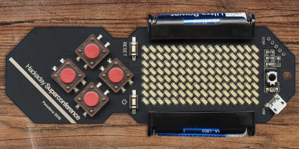
Fast forward six months — here are the modifications made to the basic concept. First, the existing LED matrix, which was composed of two compact 8×8 blocks, was replaced by 128 discrete SMD LEDs. It was a much needed change to help scale down the dimensions and clunkiness, but also to avoid another painful experience of trying to purchase and have the matrix displays shipped, which seriously threatened the production of the previous badge.

It’s a long story which I discussed in my Belgrade talk — it turned out we did not manage to get enough common anode (CA) displays from all distributors in the whole world. We had a plan B, which also fizzled, leaving us with the plan C which actually included two “C”s: Common Cathode. We cleaned up all the supplies at five distributors, and managed to get 122 CA red, 340 CC red and 78 CA green displays (enough for only 270 badges) — the entire world supply. After that, you couldn’t get any 38 mm Kingbright’s display for months! The only problem was that there were two different versions of PCBs, one for CA and the other for CC displays, but luckily only one version of software, as it could autodetect the display type.

accelerometer-on-the-boardMotion and Expansion

So, what else was new in the concept? In the Belgrade version, the badge supported an accelerometer module and included an unpopulated footprint in case you decided to install it, but now the badge has the MEMS chip LIS3 as an integral part. There are nine pads (with five I/O ports, driven directly from the MCU) to which you can add a 9-pin expansion connector. There will be a number of these connectors at the Design Lab, so that anyone can expand their badge for their convenience, on the spot.

The Visual Design

The biggest change was in the visual design. What we came up with ended up being a fair bit smaller, lighter, with a more convenient shape, and less than half the thickness of the previous one. After we had scrapped quite a few ideas during the development process (including stylized skull, frog, etc), we were left with a couple of options which you can see on the image below. The wireframe drawing on the left hand side is the Belgrade badge, shown here for a size comparison. At this point the locale and date of the conference weren’t yet definitive, which is why you see San Francisco written on the images.

design-options-2016-supercon-badge

Design number 4 prevailed, so the PCB layout could begin. I don’t like autorouted PCBs, so I was in for quite a rough time trying to solve the routing manually having only 2 layers on the board at my disposal.

Routing a Compact LED Matrix

The LED matrix is so dense that there was virtually no room on the LED layer, so most of the tracks on the component layer had to be routed as if it was a single layer PCB. To make matters worse, the LED layer is routed as a matrix, with a bunch of horizontal and vertical tracks, otherwise a good reason to use a 4-layer PCB. To stay inside the budget, everything had to be placed on 2 layers, and that’s why the final result seems so confusing at the populated area between batteries:

Continue reading “Design And Hacking Drilldown: SuperCon Badge”

It’s Time To Finally Figure Out How To Use KiCAD

KiCAD has been making leaps and bounds recently, especially since CERN is using it almost exclusively. However, while many things are the same, just enough of them are different from our regular CAD packages that it’s hard to get started in the new suite.

[Chris Gammell] runs Contextual Electronics, an online apprenticeship program which goes from concept to assembled electronics covering everything in between. To take the course you pay a nominal fee, but [Chris] posted a very excellent ten-part video series made during the last run of classes which you can watch without charge. The videos go through the basics of KiCAD while hitting the major points to consider when designing and manufacturing your electronics.

The project [Chris] chose is a simple circuit that blinks an LED with a 555. The first videos cover navigating KiCAD’s component schematic editor and library system. Next comes creating circuit schematics and component footprint creation. [Chris] covers PCB layout, the generation of Gerber files, and finally ordering the design from OSH Park — the purveyors of purple boards we’ve come to know and love. The series finishes up with simulating the circuit in LTSpice, ordering the parts, and finally soldering and debugging of the board. If all goes correctly you should now have a single blinking LED.

If the bright summer sun is burning your delicate skin, and you’d rather be locked inside with solder fumes, add this to your watch list now!

Continue reading “It’s Time To Finally Figure Out How To Use KiCAD”

KiCad Utilities Generate Parts; Track Costs

The popularity of KiCad keeps increasing, and not only are more people converting to it and using it for their projects, but there’s also a growing number of folks actively contributing to the project in the form of libraries, scripts and utilities to improve the work flow.

KiPart

[Dave Vandenbout] a.k.a [xesscorp] has written a couple of utilities for KiCad. When working with large multi pin parts such as micro-controllers, creating a schematic symbol from scratch using the traditional KiCad schematic library editor can be quite tedious. KiPart is a python script that uses a CSV table as its input to generate the KiCad schematic symbol and is able to create multi-part symbols too. Usage is quite simple. The csv file needs a part name on its first row. The next row contains the headers. ‘Pin’ number and Pin ‘Name’ are the minimum required. Additionally, you can add in ‘Unit’, ‘Side’, ‘Type’, and ‘Style’. Unit is used when defining multi-unit parts. Side decides the location of the pin, Type its function, and Style is its graphic representation. Running the KiPart python script then results in a nice KiCad schematic symbol. Besides, KiPart can specifically generate schematic symbols for the Xilinx 7-Series FPGAs and the Cypress PSoC5LP. There are a whole host of options to customize the final output, for example ordering pin placement based on pin number, or pin name or pin function. Source files can be obtained from the [xesscorp] Github repository.

KiCost

KiCost
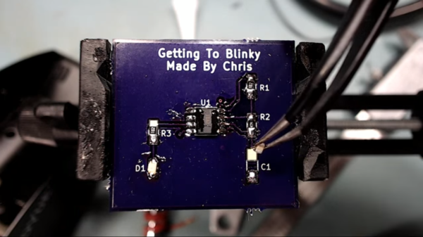
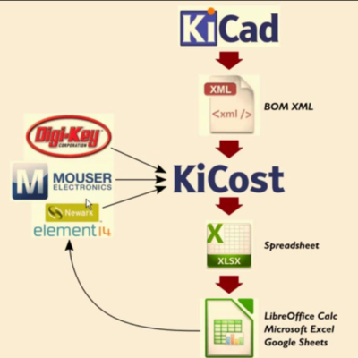
Another useful utility from [xesscorp] is KiCost. It is intended to be run as a script for generating part-cost spreadsheets for circuit boards developed with KiCad. The one piece of information you need to add to your schematic parts is a manufacturers part number. The KiCost Python script then processes the BOM XML file, reading the manufacturer part number, scraping the web sites of several popular distributors for price and inventory data, and creating a costing spreadsheet. You can grab the source files from the KiCost Github repository.

Check the two videos below where [Dave] walks through the two utilities.

Thanks to [RoGeorge] for sending in this tip by commenting on the Open Source FPGA Pi Hat built by [Dave] that we featured recently.

Continue reading “KiCad Utilities Generate Parts; Track Costs”

Best Practices To Include In Your Final Projects

electronic-best-practices

Making that final push to button up your projects can be a bit daunting. It’s kind of like the punch list on a construction project — add switch plates, fill nail holes in baseboards, screw in light bulbs, clean windows — that stuff adds up quickly. But having a set of best practices in mind throughout the development phase will cut down on that burden. [Caleb P.] just published a quick guide using a recent project as an example.

First and foremost is the label seen on the project box lid. How many times have you pulled out a circuit board from a year or two earlier and not been able to figure out the pinout? As with ancient televisions and radios, including the service schematic will save you big time! He also mentions that the size and orientation of the components in the case was in the back of his mind the whole time. That paid off because everything fits like a glove. [Caleb] makes sure the battery is easy to get to, and the each component has some type of connector so that it may be removed and serviced/replace without soldering. There’s certainly nothing groundbreaking in this guide. But ask yourself: have I been following all of these guidelines in my own work?