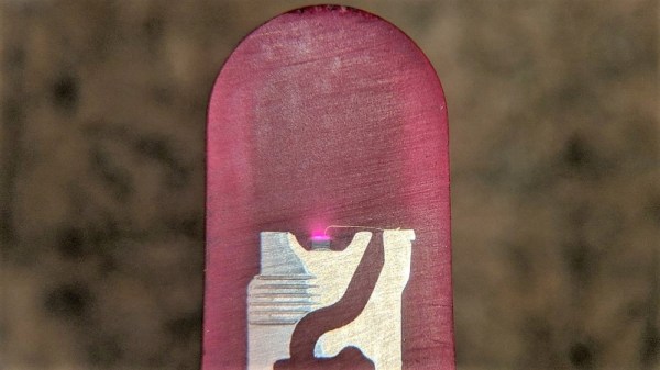
Surface-mount technology has been a fantastic force multiplier for electronics in general and for hobbyists in particular. But sometimes you’ve got no choice but to use through-hole components, meaning that even if you can take advantage of SMDs for most of the design, you still might need to spend a little time with soldering iron in hand. Or not, if you’ve got a spare 3D printer lying around.
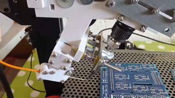
All we’ve got here is a fairly brief video from [hydrosys4], so there aren’t a lot of build details. But it’s pretty clear what’s going on here. Starting with what looks like a Longer LK4 printer, [hydrosys4] added a bracket to hold a soldering iron, and a guide for solder wire. The solder is handled by a more-or-less standard extruder, which feeds it into the joint once it’s heated by the iron. The secret sauce here is probably the fixturing, with 3D-printed jigs that hold the through-hole connectors in a pins-up orientation on the bed of the printer. With the PCB sitting on top of the connectors, it’s just a matter of teaching the X-Y-Z position of each joint, applying heat, and advancing the solder with the extruder.
The video below shows it in action at high speed; we slowed it down to 25% to get an idea of how it is in reality, and while it might not be fast, it’s precise and it doesn’t get tired. It may not have much application for one-off boards, but if you’re manufacturing small PCB runs, it’s a genius solution. We’ve seen similar solder bots before, but hats off to [hydrosys4] for keeping this one simple.
Continue reading “Modified 3D-Printer Solders Through-Hole Components”