It’s human nature to look at the technological achievements of the ancients — you know, anything before the 1990s — and marvel at how they were able to achieve precision results in such benighted times. How could anyone create a complicated mechanism without the aid of CNC machining and computer-aided design tools? Clearly, it was aliens.
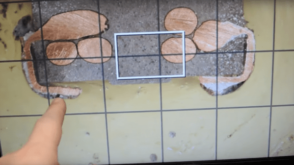
Or, as [Chris] from Click Spring demonstrates by creating precision nesting thin-wall tubing, it was human beings running the same wetware as what’s running between our ears but with a lot more patience and ingenuity. It’s part of his series of experiments into how the craftsmen of antiquity made complicated devices like the Antikythera mechanism with simple tools. He starts by cleaning up roughly wrought brass rods on his hand-powered lathe, followed by drilling and reaming to create three tubes with incremental precision bores. He then creates matching pistons for each tube, with an almost gas-tight enough fit right off the lathe.
Getting the piston fit to true gas-tight precision came next, by lapping with a jeweler’s rouge made from iron swarf recovered from the bench. Allowed to rust and ground to a paste using a mortar and pestle, the red iron oxide mixed with olive oil made a dandy fine abrasive, perfect for polishing the metal to a high gloss finish. Making the set of tubes concentric required truing up the bores on the lathe, starting with the inner-most tube and adding the next-largest tube once the outer diameter was lapped to spec.
Easy? Not by a long shot! It looks like a tedious job that we suspect was given to the apprentice while the master worked on more interesting chores. But clearly, it was possible to achieve precision challenging today’s most exacting needs with nothing but the simplest tools and plenty of skill. Continue reading “Clickspring’s Experimental Archaeology: Concentric Thin-Walled Tubing”
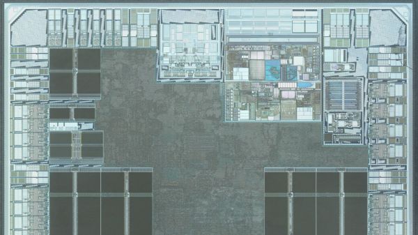

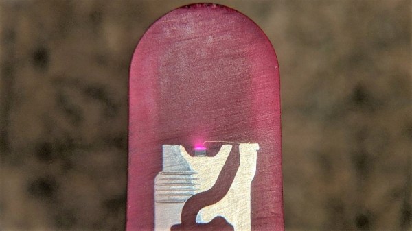
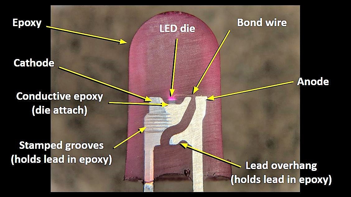
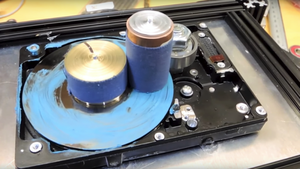
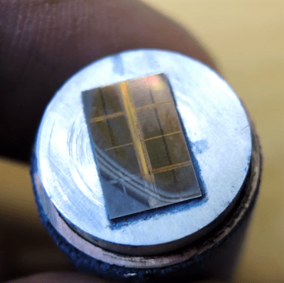 For those not into the anatomy and physiology of semiconductors, getting a look at the inside of the chip can reveal valuable information needed to reverse engineer a device, or it can just scratch the itch of curiosity. Lapping (the gentle grinding away of material) is one way to see the layers that make up the silicon die that lies beneath the epoxy. Hard drives designed to spin at 7200 rpm or more hardly seem a suitable spinning surface for a gentle lapping, but [electronupdate] just wanted the platter for its ultra-smooth, ultra-flat surface.