There are a range of integrated circuits that most of us would regard as definitive examples of their type, devices which became the go-to for a particular function and which have entered our collective consciousness as electronics enthusiasts. They have been in production since the early days of consumer integrated circuits, remaining in use because of a comprehensive understanding of their characteristics among engineers, and the job they do well.
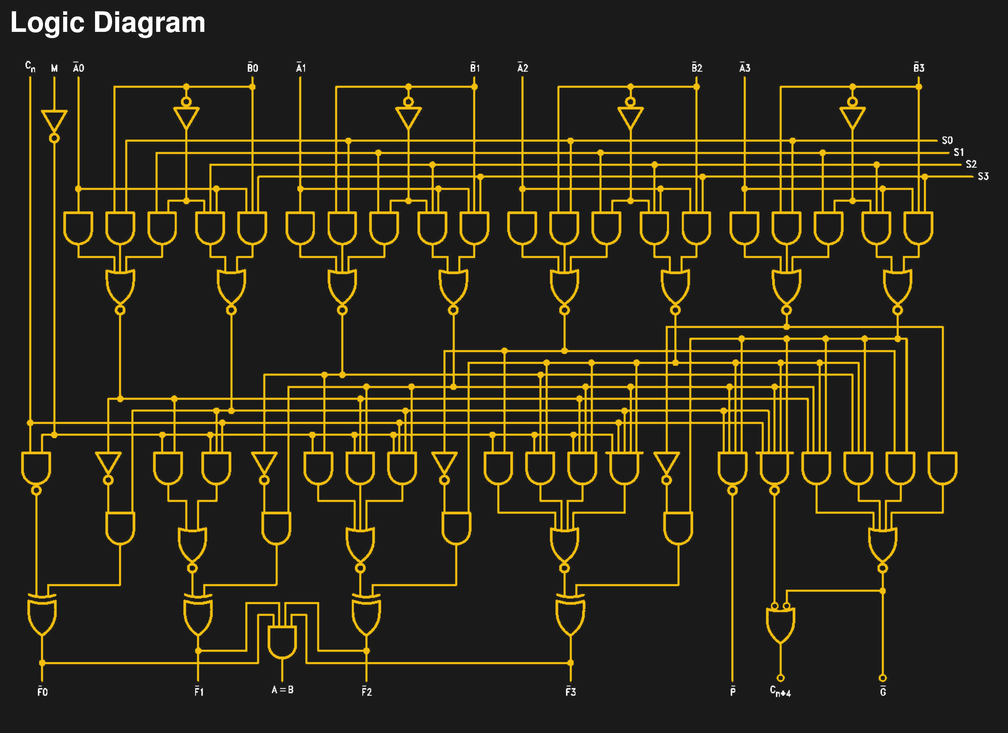
You can probably name the ones I’m going to rattle off here, the µA741 op-amp designed by David Fullagar for Fairchild in 1968, the NE555 timer from Hans Camenzind for Signetics in 1971, and a personal favourite, Bob Widlar’s µA723 linear regulator for Fairchild in 1967. There may be a few others that readers will name in the comments, but there’s one that until today it’s likely that few of you would have considered. Texas Instruments’ 5400 and 7400 TTL quad 2-input NAND gate has been in continuous production since 1964 and is the progenitor of what is probably the most numerous breed of integrated circuits, yet it doesn’t trip off the tongue when listing famous chips, and none of us can name its designer. So today we’re turning the spotlight on this neglected piece of silicon, and trying to bring it the adulation it deserves. Continue reading “The 7400 Quad 2-Input NAND Gate, A Neglected Survivor From A Pre-Microprocessor World”