Design And Hacking Drilldown: SuperCon Badge

One can imagine a political or business conference without an interactive badge — but not a hacker conference. Does this make the case for hackers being a special breed of people, always having something creative to show for their work? Yes, I think it does.

Following the Hackaday Belgrade conference in April of this year, we met at the Supplyframe offices to discuss the badge for the Hackaday SuperConference that will happen in Pasadena on 5+6th of November. The Belgrade conference badge (which was fully documented if you’re curious) was surprisingly popular, and I was asked to design the new one as well.

I was prepared to come up with something completely new, but [Mike Szczys] suggested keeping with the same basic concept for the project: “No reason to change anything, we have a badge that works”. To which I responded: “Well, the next one will also work”. But then I realized that “works” does not stand for “being functional”. The key is that it was embraced by visitors who played with it, coded on it, and solved a crypto challenge with it.

The World Doesn’t Have Enough LEDs

led-modules-versus-smd
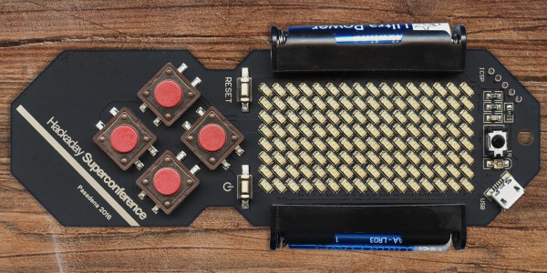
Fast forward six months — here are the modifications made to the basic concept. First, the existing LED matrix, which was composed of two compact 8×8 blocks, was replaced by 128 discrete SMD LEDs. It was a much needed change to help scale down the dimensions and clunkiness, but also to avoid another painful experience of trying to purchase and have the matrix displays shipped, which seriously threatened the production of the previous badge.

It’s a long story which I discussed in my Belgrade talk — it turned out we did not manage to get enough common anode (CA) displays from all distributors in the whole world. We had a plan B, which also fizzled, leaving us with the plan C which actually included two “C”s: Common Cathode. We cleaned up all the supplies at five distributors, and managed to get 122 CA red, 340 CC red and 78 CA green displays (enough for only 270 badges) — the entire world supply. After that, you couldn’t get any 38 mm Kingbright’s display for months! The only problem was that there were two different versions of PCBs, one for CA and the other for CC displays, but luckily only one version of software, as it could autodetect the display type.

accelerometer-on-the-boardMotion and Expansion

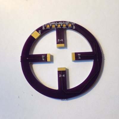
So, what else was new in the concept? In the Belgrade version, the badge supported an accelerometer module and included an unpopulated footprint in case you decided to install it, but now the badge has the MEMS chip LIS3 as an integral part. There are nine pads (with five I/O ports, driven directly from the MCU) to which you can add a 9-pin expansion connector. There will be a number of these connectors at the Design Lab, so that anyone can expand their badge for their convenience, on the spot.

The Visual Design

The biggest change was in the visual design. What we came up with ended up being a fair bit smaller, lighter, with a more convenient shape, and less than half the thickness of the previous one. After we had scrapped quite a few ideas during the development process (including stylized skull, frog, etc), we were left with a couple of options which you can see on the image below. The wireframe drawing on the left hand side is the Belgrade badge, shown here for a size comparison. At this point the locale and date of the conference weren’t yet definitive, which is why you see San Francisco written on the images.

design-options-2016-supercon-badge

Design number 4 prevailed, so the PCB layout could begin. I don’t like autorouted PCBs, so I was in for quite a rough time trying to solve the routing manually having only 2 layers on the board at my disposal.

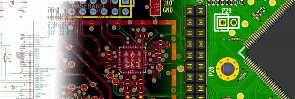
Routing a Compact LED Matrix

The LED matrix is so dense that there was virtually no room on the LED layer, so most of the tracks on the component layer had to be routed as if it was a single layer PCB. To make matters worse, the LED layer is routed as a matrix, with a bunch of horizontal and vertical tracks, otherwise a good reason to use a 4-layer PCB. To stay inside the budget, everything had to be placed on 2 layers, and that’s why the final result seems so confusing at the populated area between batteries:

Continue reading “Design And Hacking Drilldown: SuperCon Badge”

It’s Time To Finally Figure Out How To Use KiCAD

KiCAD has been making leaps and bounds recently, especially since CERN is using it almost exclusively. However, while many things are the same, just enough of them are different from our regular CAD packages that it’s hard to get started in the new suite.

[Chris Gammell] runs Contextual Electronics, an online apprenticeship program which goes from concept to assembled electronics covering everything in between. To take the course you pay a nominal fee, but [Chris] posted a very excellent ten-part video series made during the last run of classes which you can watch without charge. The videos go through the basics of KiCAD while hitting the major points to consider when designing and manufacturing your electronics.

The project [Chris] chose is a simple circuit that blinks an LED with a 555. The first videos cover navigating KiCAD’s component schematic editor and library system. Next comes creating circuit schematics and component footprint creation. [Chris] covers PCB layout, the generation of Gerber files, and finally ordering the design from OSH Park — the purveyors of purple boards we’ve come to know and love. The series finishes up with simulating the circuit in LTSpice, ordering the parts, and finally soldering and debugging of the board. If all goes correctly you should now have a single blinking LED.

If the bright summer sun is burning your delicate skin, and you’d rather be locked inside with solder fumes, add this to your watch list now!

Continue reading “It’s Time To Finally Figure Out How To Use KiCAD”

Beautiful And Bizarre Boards

weirdboard
An odd board (piezo coupler), fabbed by OSHPark.

Recently I’ve been getting curious about interesting PCB shapes. In the past I’ve always used simple Polygons, perhaps rounding out the corners to make the design a little more aesthetically pleasing. The board to the right was my introduction to the possibilities of oddly shaped boards. It’s designed to couple with a piezo buzzer (used as an actuator). I’ve been planning to have it fabricated out of FPC (Flexible Printed Circuits), but with fabrication being so cheap I sent it to OSHPark to see what they’d make of it. OSHPark doesn’t have hard specs around internal routing, but in my experience they’re up to try anything (and they’re quality is always great). The width of the prongs on the PCB shown is 5mm. I figured it was a risk, and that it was likely the FR4 could break, but it came back great!

This has led me to the realization that my boards could look much more exciting than they do currently, and that our highly optimized modern PCB fabrication process provides a lot of room for experimentation. This article will discuss some of the options available when creating non-traditional PCBs.

Continue reading “Beautiful And Bizarre Boards”

Pack Your Plywood Cuts With Genetic Algortihms

Reading (or writing!) Hackaday, we find that people are often solving problems for us that we didn’t even know that we had. Take [Jack Qiao]’s SVGnest for instance. If you’ve ever used a laser cutter, for instance, you’ve probably thought for a second or two about how to best pack the objects into a sheet, given it your best shot, and then moved on. But if you had a lot of parts, and their shapes were irregular, and you wanted to minimize materials cost, you’d think up something better.

SVGnest, which runs in a browser, takes a bunch of SVG shapes and a bounding box as an input, and then tries to pack them all as well as possible. Actually optimizing the placement is a computationally expensive proposition, and that’s considering the placement order to be fixed and allowing only 90 degree rotations of each piece.

Once you consider all the possible orders in which you place the pieces, it becomes ridiculously computationally expensive, so SVGnest cheats and uses a genetic algorithm, which essentially swaps a few pieces and tests for an improvement many, many times over. Doing this randomly would be silly, so the routine packs the biggest pieces first, and then back-fills the small ones wherever they fit, possibly moving the big ones around to accommodate.

That’s a lot of computational work, but the end result is amazing. SVGnest packs shapes better than we could ever hope to, and as well as some commercial nesting software. Kudos. And now that the software is written, as soon as you stumble upon this problem yourself, you have a means to get to the solution. Thanks [Jack]!

KiCad 4.0 Is Released

If you’re a KiCad user, as many of us here at Hackaday are, you’ll be elated to hear that KiCad 4.0 has just been released! If you’re not yet a KiCad user, or if you’ve given it a shot in the past, now’s probably a good time to give it a try. (Or maybe wait until the inevitable 4.0.1 bugfix version comes out.)

If you’ve been using the old “stable” version of KiCad (from May 2013!), you’ve got a lot of catching-up to do.

The official part footprint libraries changed their format sometime in 2014, and are all now hosted on GitHub in separate “.pretty” folders for modularity and ease of updating. Unfortunately, this means that you’ll need to be a little careful with your projects until you’ve switched all the parts over. The blow is softened by a “component rescue helper” but you’re still going to need to be careful if you’re still using old schematics with the new version.

The most interesting change, from a basic PCB-layout perspective, is the push-and-shove router. We’re looking for a new demo video online, but this one from earlier this year will have to do for now. We’ve been using various “unstable” builds of KiCad for the last two years just because of this feature, so it’s awesome to see it out in an actual release. The push-and-shove router still has some quirks, and doesn’t have all the functionality of the original routers, though, so we often find ourselves switching back and forth. But when you need the push-and-shove feature, it’s awesome.

If you’re doing a board where timing is critical, KiCad 4.0 has a bunch of differential trace and trace-length tuning options that are something far beyond the last release. The 3D board rendering has also greatly improved.

Indeed, there are so many improvements that have been made over the last two and a half years, that everybody we know has been using the nightly development builds of KiCad instead of the old stable version. If you’ve been doing the same, version 4.0 may not have all that much new for you. But if you’re new to KiCad, now’s a great time to jump in.

We’ve covered KiCad hacks before, and have another article on KiCad add-on utilities in the pipeline as we write this. For beginners, [Chris Gammell]’s tutorial video series is still relevant, and is a must-watch.

Thanks [LC] for the newsworthy tip!

KiCad Video Series: From Concept To Manufacture

Many of our readers took the habit of using Eagle to design their PCBs. Even if you’ll find plenty of support for this software as well as a lot of parts libraries, the software comes with limitations. The useable board area is limited to 4×3.2 inches, only two signal layers can be used and more importantly the schematics editor can only create one sheet. On the other side, some of you may already know KiCad, a free open source and unrestricted schematics and layout software. [Chris] just tipped us of a video series he made, showing people how to design and build their very first PCB using this software. It’s a simple 555 circuit, but goes through all the steps necessary to design a PCB that costs only $5 through OSHpark… and will blink by the end. All the videos are also embedded after the break.

Continue reading “KiCad Video Series: From Concept To Manufacture”

Comparing Altium And Cadence PCB Layout Tools

We see a lot of projects using Eagle for the schematics and PCB layout. There are a few that use Kicad, but we hear very little about other alternatives. Recently, [Limpkin] has been working with Altium and Cadence and wrote about how they compare when it comes to PCB layout. Neither are free packages so it’s good to know what you’re getting into before taking the plunge.

[Limpkin] begins his overview by mentioning that the schematic editors are comparable; the differences start to show themselves in the PCB layout tools. Here you can see that Altium always labels the pads so you know what net each of them belongs to. Cadence (whose PCB layout tool is called Allegro) will display the net if you hover over the pad with your mouse. Both have 3D rendering, with Altium’s looking a bit more pleasant but what real use is it anyway? Okay, we will admit we love a good photorealistic board rendering, but we digress. The most interesting differences show themselves once traces are all on the board and need to be rejiggered. Cadence will actually move traces on other layers automatically to avoid collision with a via that is late to the party, and Altium shows some strange behavior when dragging traces. [Limpkin] doesn’t register a final judgement, but the comparison alone is worth the read.