Bit Of OpenSCAD Code Caps Off Wiremold

Wiremold is great stuff — it’s relatively cheap, easy to work with, and offers all sorts of adapters and angle pieces which take the hassle out of running (and hiding) wires. But [Dr. Gerg] found a shortcoming of this otherwise very flexible product: since each run is intended to start and end in a surface mounted box, he couldn’t find an end cap that would let him close off a section.

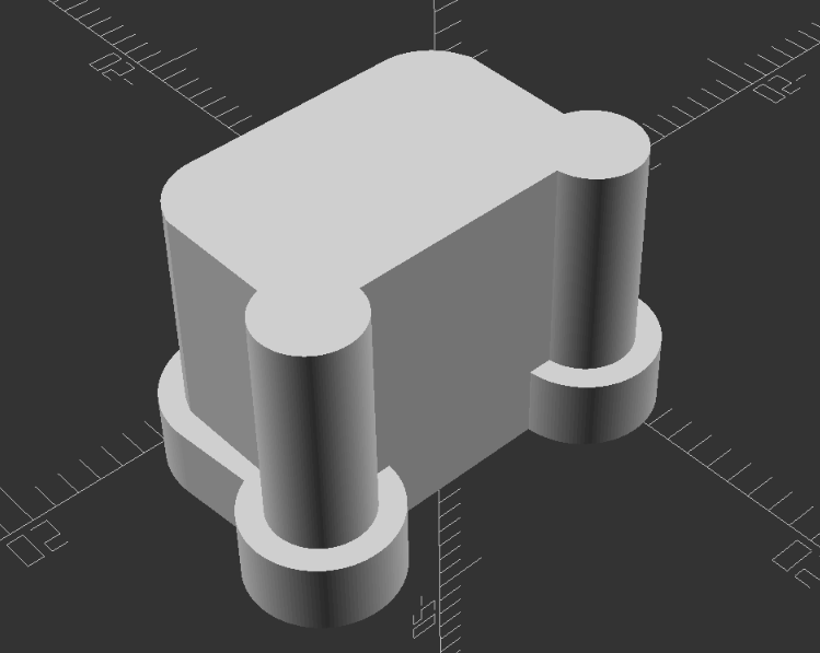
The solution? A desktop 3D printer and a chunk of OpenSCAD code telling it what to extrude. When you break it down, the Wiremold profile is fairly straightforward, and can be easily described with geometric primitives. A handful of cylinders, a cube or two, tie it all together with the hull() function, and you’re there.

We’d say this would be a fantastic project to cut your OpenSCAD teeth on, but since [Dr. Gerg] was kind enough to share the source code, you don’t have to figure it out on your own. Though there’s still benefit in reading over it if you’re looking for some practical examples of how the “Programmers Solid 3D CAD Modeller” gets things done.

So why would you want a Wiremold endcap? In the case of [Dr. Gerg], it sounds like he was trying to cover up a short run of wire that was running vertically. But we could imagine other applications for this basic design now that it’s out in the wild. For example, a short length of Wiremold outfitted with a pair of printed caps could make for a nice little enclosure if you’ve got a small project that needs protecting.

Kernel Hack Brings Windows XP To The 486

The venerable Intel 486 was released in 1989 as the successor to the extremely popular Intel 386. It was the minimum recommended processor for Windows 98.  (Surprisingly, the Windows 95 minimum was a 386!)  But by the time XP rolled around, you needed at least a 233 MHz Pentium to install. Or at least that was the case until recently when an extremely dedicated user on MSFN named [Dietmar] showed how he hacked the XP kernel so it could run on the classic chip!

The biggest issue preventing XP from working on earlier processors is an instruction introduced on the Pentium: CMPXCHG8B. This instruction compares two 8-byte values and takes different actions depending on an equality test. It either copies the 8 bytes to a destination address or loads it into a 64-bit register. Essentially, it does what it says on the tin: it CoMPares and eXCHanGes some values. If you want to dig into the nitty-gritty details, you can check out this info on the instruction taken from the x86 datasheet.

Without getting too technical, know that this instruction is vital for performance when working with large data structures. This is because one instruction moves 8 bytes at a time, unlike the older CMPXCHG instruction, which only moves a single byte. Essentially, [Dietmar] had to find every usage of CMPXCHG8B and replace it with an equivalent series of CMPXCHG instructions.

On a side note, the once well-known and devastating Pentium F00F bug was caused by a faulty encoding of the CMPXCHG8B instruction. This allowed any user, even unprivileged users, to completely lock up a system, requiring a full reset cycle!

So [Dietmar] was successful, and now you can run the German version of Windows XP on either a real 486 or an emulated one. The installer is available on the Internet Archive and there’s a detailed video below demonstrating installing it on the 86Box virtual machine host.

Continue reading “Kernel Hack Brings Windows XP To The 486”

Hackaday Links Column Banner

Hackaday Links: June 23, 2024

When a ransomware attack targets something like a hospital, it quickly becomes a high-profile event that understandably results in public outrage. Hospitals are supposed to be backstops for society, a place to go when it all goes wrong, and paralyzing their operations for monetary gain by taking over their information systems is just beyond the pale. Tactically, though, it makes sense; their unique position in society seems to make it more likely that they’ll pay up.

Which is why the ongoing cyberattack against car dealerships is a little perplexing — can you think of a less sympathetic victim apart from perhaps the Internal Revenue Service? Then again, we’re not in the ransomware business, so maybe this attack makes good financial sense. And really, judging by the business model of the primary target of these attacks, a company called CDK Global, it was probably a smart move. We had no idea that there was such a thing as a “Dealer Management System” that takes care of everything from financing to service, and that shutting down one company’s system could cripple an entire industry, but there it is.

Continue reading “Hackaday Links: June 23, 2024”

The Best DIY PCB Method?

Now before you start asking yourself “best for what purpose?”, just have a look at the quality of the DIY PCB in the image above. [ForOurGood] is getting higher resolution on the silkscreen than we’ve seen in production boards. Heck, he’s got silkscreen and soldermask at all on a DIY board, so it’s definitely better than what we’re producing at home.

The cost here is mostly time and complexity. This video demonstrating the method is almost three hours long, so you’re absolutely going to want to skip around, and we’ve got some relevant timestamps for you. The main tools required are a cheap 3018-style CNC mill with both a drill and a diode laser head, and a number of UV curing resins, a heat plate, and some etchant.

[ForOurGood] first cleans and covers the entire board with soldermask. A clever recurring theme here is the use of silkscreens and a squeegee to spread the layer uniformly. After that, a laser removes the mask and he etches the board. He then applies another layer of UV soldermask and a UV-curing silkscreen ink. This is baked, selectively exposed with the laser head again, and then he cleans the unexposed bits off.

In the last steps, the laser clears out the copper of the second soldermask layer, and the holes are drilled. An alignment jig makes sure that the drill holes go in exactly the right place when swapping between laser and drill toolheads – it’s been all laser up to now. He does a final swap back to the laser to etch additional informational layers on the back of the board, and creates a solder stencil to boot.

This is hands-down the most complete DIY PCB manufacturing process we’ve seen, and the results speak for themselves. We would cut about half of the corners here ourselves. Heck, if you do single-sided SMT boards, you could probably get away with just the first soldermask, laser clearing, and etching step, which would remove most of the heavy registration requirements and about 2/3 of the time. But if it really needs to look more professional than the professionals, this video demonstrates how you can get there in your own home, on a surprisingly reasonable budget.

This puts even our best toner transfer attempts to shame. We’re ordering UV cure soldermask right now.

Continue reading “The Best DIY PCB Method?”

Rescued IMac G4 Restored And Upgraded With Mac Mini M1 Guts

Three abandoned iMac G4s, looking for a loving home... (Credit: Hugh Jeffreys)
Three abandoned iMac G4s, looking for a loving home… (Credit: Hugh Jeffreys)

The Apple iMac G4 was also lovingly referred to as the ‘Apple iLamp’ due to its rather unique design with the jointed arm on which the display perches. Released in 2002 and produced until 2004, it was the first iMac to feature an LCD. With only a single-core G4 PowerPC CPU clocked at around 1 GHz, they’re considered e-waste by the average person.

That’s how [Hugh Jeffreys] recently found a triplet of these iMacs abandoned at an industrial site. Despite their rough state, he decided to adopt them on the spot, and gave one of them a complete make-over, with a good scrub-down and a brand-new LCD and Mac Mini M1 guts to replace the broken G4 logic board.

The chosen iMac had a busted up screen and heavily corroded logic board that looked like someone had tried to ‘fix’ it before. A new (used) 17″ LCD was installed from a MacBook Pro, which required the use of a Realtek RTD2660-based display controller to provide HDMI to LVDS support. The new logic board and power supply were sourced from a Mac Mini featuring the M1 SoC, which required a 3D printed adapter plate to position everything inside the iMac’s base. Wiring everything up took some creative solutions, with routing the wires through the flexible monitor arm the biggest struggle. The WiFi antenna on the Mac Mini turned out to be riveted and broke off, but the iMac’s original WiFi antenna could be used instead.

Although some clean-up is still needed, including better internal connector extensions, the result is a fully functional 2024 iMac M1 that totally wouldn’t look out of place in an office today. Plus it’s significantly easier to adjust the monitor’s angle and height compared to Apple’s official iMac offerings, making it the obviously superior system.

Continue reading “Rescued IMac G4 Restored And Upgraded With Mac Mini M1 Guts”

TSMC’s Long Path From Round To Square Silicon Wafers

Crystal of Czochralski-grown silicon.

Most of us will probably have seen semiconductor wafers as they trundle their way through a chip factory, and some of us may have wondered about why they are round. This roundness is an obvious problem when one considers that the chip dies themselves are rectangular, meaning that a significant amount of the dies etched into the wafers end up being incomplete and thus as waste, especially with (expensive) large dies. This is not a notion which has escaped the attention of chip manufacturers like TSMC, with this particular manufacturer apparently currently studying a way to make square substrates a reality.

According to the information provided to Nikkei Asia by people with direct knowledge, currently 510 mm x 515 mm substrates are being trialed which would replace the current standard 12″ (300 mm) round wafers. For massive dies such as NVidia’s H200 (814 mm2), this means that approximately three times as many would fit per wafer. As for when this technology will go into production is unknown, but there exists significant incentive in the current market to make it work.

As for why wafers are round, this is because of how these silicon wafers are produced, using the Czochralski method, named after Polish scientist [Jan Czochralski] who invented the method in 1915. This method results in rod-shaped crystals which are then sliced up into the round wafers we all know and love. Going square is thus not inherently impossible, but it will require updating every step of the process and the manufacturing line to work with this different shape.

Fixed Point Math Exposed

If you are used to writing software for modern machines, you probably don’t think much about computing something like one divided by three. Modern computers handle floating point quite well. However, in constrained systems, there is a trap you should be aware of. While modern compilers are happy to let you use and abuse floating point numbers, the hardware is often woefully slow. It also tends to eat up lots of resources. So what do you do? Well, as [Low Byte Productions] explains, you can opt for fixed-point math.

In theory, the idea is simple. Just put an arbitrary decimal point in your integers. So, for example, if we have two numbers, say 123 and 456, we could remember that we really mean 1.23 and 4.56. Adding, then, becomes trivial since 123+456=579, which is, of course, 5.79.

Continue reading “Fixed Point Math Exposed”