Logic Analyzers For FPGAs: A Verilog Odyssey

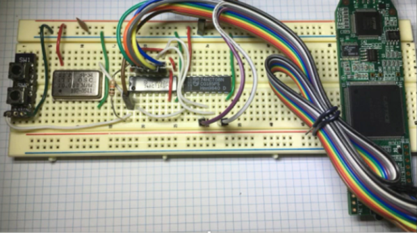
Sometimes you start something simple and then it just leads to a chain reaction of things. I wanted to write a post about doing state machines in Verilog and target the Lattice iCEstick board that we often use for quick FPGA projects. That led to a small problem: how do you show what’s going on inside? In this series of posts, we’ll look at building a logic analyzer into an FPGA to help debug itself, instantiating memory, and — finally — state machines.

Logic analysis is a common tool in FPGA development. If you use Altera, they have Signal Tap available that lets you build a simple logic analyzer into the FPGA that talks back to your PC. Xilinx has ChipScope which is about the same. Sometimes those tools either cost money or are limited in some way in the free versions. I have my sights set on a tool that can be used with the Lattice architecture.

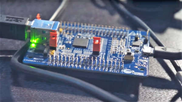
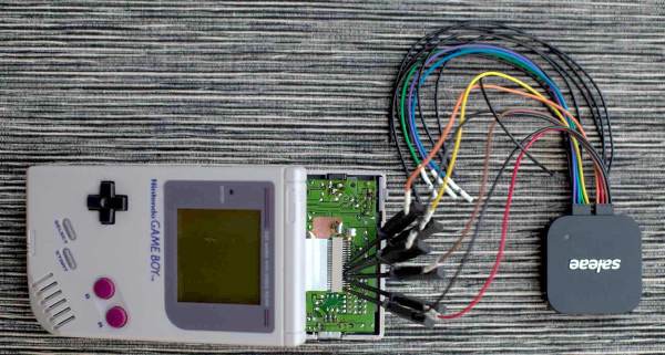
Sure, you can ship data out on I/O pins and then use a regular logic analyzer to pick up the data. But that isn’t very handy. So I thought about writing a generic logic analyzer component. But before I did I decided to check to see if someone else had already done it.

Spoiler alert: they did, but I wanted something a little different so I wound up extending the program significantly. What I wound up with is a reasonably portable Verilog logic analyzer that can produce traces like this one:

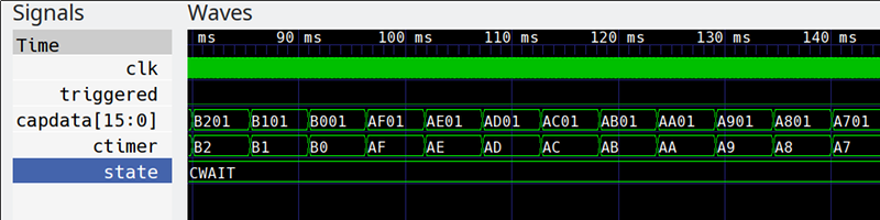
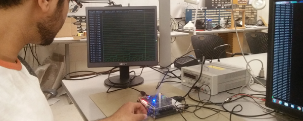
Keep in mind, this isn’t a simulation. This is real data pulled off the actual FPGA. Yes, that is gtkwave producing the plots, but the input data is a VCD file generated from samples taken inside the FPGA.

Continue reading “Logic Analyzers For FPGAs: A Verilog Odyssey”

Spite, Thrift, And The Virtues Of An Affordable Logic Analyzer

[Larry Wall], the father of Perl, lists the three great virtues of all programmers: Laziness, Impatience, and Hubris. After seeing that Saleae jacked up the prices on their popular logic analyzers to ludicrous levels, [CNLohr] added a fourth virtue: Spite. And since his tests with a Cypress FX3 over the last few days may lead to a dirt-cheap DIY logic analyzer, we may soon be able to add another virtue: Thrift.

The story begins a year or two ago when [CNLohr] got a Cypress FX3 development board for $45. The board sat unused for want of a Windows machine, but after seeing our recent article on a minimalist logic analyzer based on an FX2, he started playing with the board to see if it could fan the flames of his Saleae hatred. The FX3 is a neat little chip that has a 100-MHz General Programmable Interface (GPIF) bus that basically lets it act like an easy to use FPGA.

Prepared to spend months on the project, he was surprised to make significant progress on his mission of spiteful thrift within a few days, reading 16 bits off the GPIF at over 200 megabytes per second and dumping it over the USB 3.0 port. [Charles]’ libraries for the FX3 lay the foundation for a lot of cool stuff, from logic analyzers to SDRs and beyond — now someone just has to build them.

The search for a cheap but capable logic analyzer is nothing new, of course. Last year, both [Jenny List] and [Bil Herd] looked at the $22 iCEstick as a potential Saleae beater.

Continue reading “Spite, Thrift, And The Virtues Of An Affordable Logic Analyzer”

Old Logic Analyzer Becomes New PC Case

There are a lot of cool ways to wrap a case around your custom PC build. But the off-the-shelf stuff doesn’t really set your machine apart from the herd, no matter how many RGB LEDs you put inside. If you really want to stand out, think out of the box, and build your PC into the case of an old logic analyzer.

Looking for a little retro cool factor, [Bob Alexander] turned to the world’s boneyard, eBay, and rounded up a dead H-P 1653 logic analyzer. State of the art in 1989 but not worth repairing by [Bob]’s lights, he removed the original 10″ CRT to make room for an alternate display. After a bit of experimentation, he settled on an LCD panel mounted behind a sheet of acrylic that he thermoformed to the shape of the CRT face. All the original guts were removed to make way for the motherboard and power supply, and a custom PCB to interface the original keypad and rotary encoder into the PC. The old buttons now launch various programs and the encoder acts as the PC volume control. The floppy drive made way for a USB hub, the BNC connectors became power and reset buttons, and a photo taken through the CRT bezel before the electronics were removed provides a window into the soul of the original instrument. It’s a really nice build, and totally unique.

Need some inspiration for your custom case mod? This wall-mounted render farm is pretty snazzy. Or perhaps you’d prefer something more apocalyptic, like this ammo can PC.

Logic Analyzer Pushes The Limits Of Miniaturization

Careful not to sneeze while using this diminutive logic analyzer — you could send it flying across the bench.

Undertaken more for the challenge than as a practical bench tool, [Uwe Hermann]’s tiny logic analyzer is an object lesson on getting a usable circuit as small as possible. Sure, some sacrifices had to be made; it’s only an eight-channel instrument without any kind of input protection at all, and lacks niceties like an EEPROM. But that allows it to fit on a mere 11 x 11-mm fleck of PCB. That’s a pretty impressive feat of miniaturization, given that the Cypress microcontroller running the show is in QFN package that takes up 64-mm² all by itself. A micro-USB connector takes up much of the back side of the board and allows the analyzer to talk to sigrok, an open-source signal analysis suite.

Everything about the project is totally open, including the PCB files, so you can build your own if you feel up to the challenge. We’d strongly suggest you check out this primer on logic analyzers first, though, especially since it focuses on the capabilities of the sigrok suite.

Using A Logic Analyzer To Generate Screenshots From A Game Boy

Wouldn’t you like to go back to a dead handheld and extract the proof of your 90s-era high scores? Of course you would.

[svendahlstrand] bought his first logic analyzer, a Logic 8 from Saleae and decided to play around with an old Game Boy. He opened up the handheld with a tri-point screwdriver and hooked six wires up to the LCD data bus, generating screen shots from the logged data. He got screens from Solomon’s Club, Mole Mania, Kid Dracula, and more.

The first few attempts were fraught with mishap as [sven] worked to figure out the settings of his new analyzer. In one instance he had the DATA 0 and DATA 1 signals reversed, also reversing two of the gray values. After figuring it out he posted his LCD sniffing tutorial to GitHub, where he also has a C program for manually piecing together the screen shots, pixel by pixel.

Thanks to [sven] for posting this project to our recent Everything You Need to Know About Logic Probes post.


Logic Analyzer On Chips

The Internet is full of low-speed logic analyzer designs that use a CPU. There are also quite a few FPGA-based designs. Both have advantages and disadvantages. FPGAs are fast and can handle lots of data at once. But CPUs often have more memory and it is simpler to perform I/O back to, say, a host computer. [Mohammad] sidestepped the choice. He built a logic analyzer that resides partly on an FPGA and partly on an ARM processor.

In fact, his rationale was to replace built-in FPGA logic analyzers like Chipscope and SignalTap. These are made to coexist with your FPGA design, but [Mohammad] found they had limitations. They also eat up die space you might want for your own design, so by necessity, they probably don’t have much memory.

The system can capture and display 32-bit signals on a 640×480 VGA monitor in real-time. The system also has a USB mouse interface which is used to zoom and scroll the display. You can see a video of the thing in operation, below.

Continue reading “Logic Analyzer On Chips”

Compiling A $22 Logic Analyzer

On my way to this year’s Hackaday SuperConference I saw an article on EE Times about someone taking the $22 Lattice iCEstick and turning it into a logic analyzer complete with a Python app to display the waveforms. This jumped out as pretty cool to me given that there really isn’t a ton of RAM on the stick, basically none that isn’t contained in the FPGA itself.

[Jenny List] has also written about the this application as created by [Kevin Hubbard] of Black Mesa Labs and [Al Williams] has a great set of posts about using this same $22 evaluation board doing ground up Verilog design using open source tools. Even if you don’t end up using the stick as a logic analyzer over the long haul, it’ll be very easy to find many other projects where you can recompile to invent a new purpose for it.

Continue reading “Compiling A $22 Logic Analyzer”