Remoticon Video: Basics Of RF Emissions Debugging Workshop

These days we’re surrounded by high-speed electronics and it’s no small feat that they can all play nicely in near proximity to each other. We have RF emissions standards to thank, which ensure new products don’t spew forth errant signals that would interfere with the data signals traveling through the ether. It’s long been the stuff of uber-expensive emissions testing labs, and failure to pass can leave you scratching your head. But as Alex Whittimore shows in this workshop from the 2020 Hackaday Remoticon, you can do a lot of RF emissions debugging with simple and inexpensive tools.

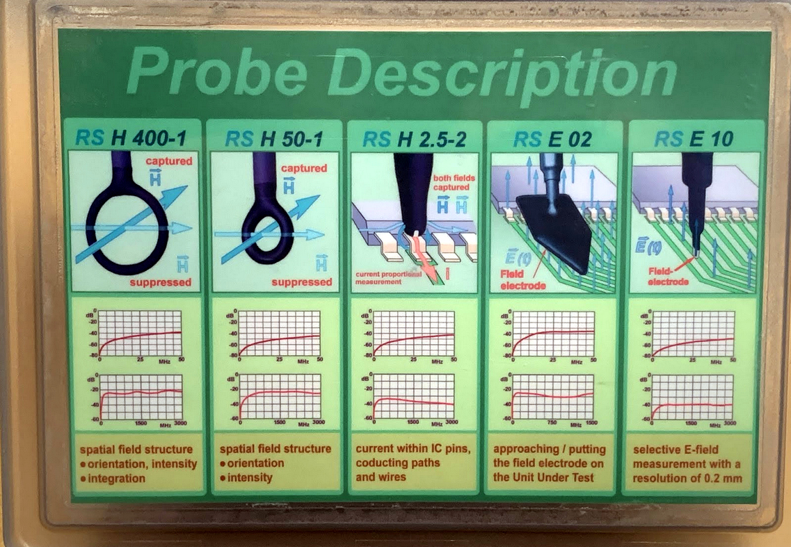
Professionally-made probes in several sizes
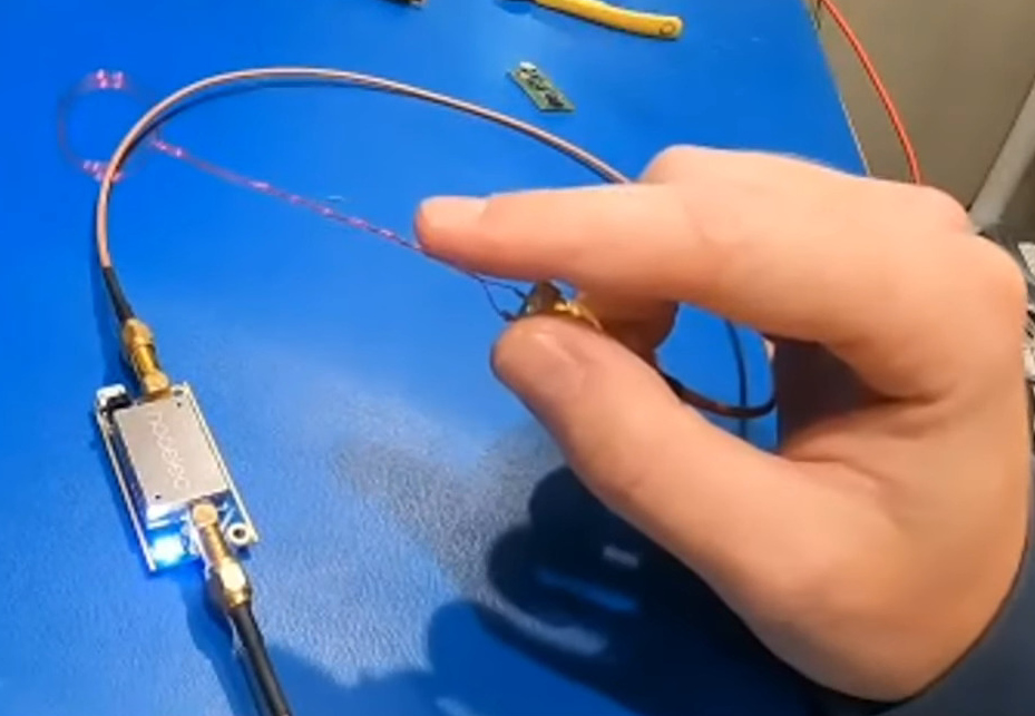
Build your own probes from magnet wire

You can get a surprisingly clear picture of what kind of RF might be coming off of a product by probing it on your own workbench. Considering the cost of the labs performing FCC and other certifications, this is a necessary skill for anyone who is designing a product headed to market — and still damn interesting for everyone else. Here you can see two examples of the probes used in the process. Although one is a pack of professional tools and other is a bit of enameled wire (magnet wire), both are essentially the same: a loop of wire on which a magnetic field will induce a very small current. Add a Low-Noise Amplifier (LNA) and you’ll be up and measuring in no-time.

I really enjoyed how Alex started his demo with “The Right WayTM” of doing things — using a proper spectrum analyzer to visualize data from the probes. But the real interesting part is “The Hacker WayTM” which leverages an RTL-SDR dongle and some open-source software to get the same job done. Primarily that means using SDRAngel and QSpectrumAnalyzer which are both included in the DragonOS_LTS which can be run inside of a virtual machine.
Continue reading “Remoticon Video: Basics Of RF Emissions Debugging Workshop”

Remoticon Video: Meta_Processing Is A Mashup Of Text And Block Programming

Very few people want to invent the universe before they blink their first LED. Sure, with enough interest a lot of folks will drill-down to the atomic level of technology and build their way back up. But there’s something magical about that first time you got your blinky to blink, and knowing how to write makefiles plays no part in that experienc). Now apply that to projects using smartphone as wireless interfaces… how simple can we make it for people?

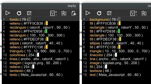
Meta_Processing can translate the instructions into any of 14 languages

Jose David Cuartas is working to answer that very question and gives us a guided tour of his progress in this Meta_Processing workshop held during the Hackaday Remoticon. Meta-Processing is an IDE based on — as you’ve probably guessed — Processing, the programming language that unlocked higher-level functionality to anyone who wanted to perform visually-interesting things without becoming software zen masters. The “Meta_” part here is that it can now be done with very limited typing and interchangeably between different spoken languages.

The approach is to take the best of text programming and block programming languages and mash them together. In that way, you don’t type new lines, you add them with a click of the mouse and select the instruction you want to use on that line from a list. It means you don’t need to have the instructions memorized, and avoids typos in your code. The docs for that instruction will be shown on the bottom bar of the IDE to help you with parameters. And the kicker is that since you’re selecting the instructions, choosing any of the IDE’s 14 available spoken languages will update your “code” with translations into the new language.

In the workshop, video of which is included below, Jose demonstrates a number if interesting examples including audio, video, and user input, using a surprisingly small amount of code. The IDE even spawns a server on the network so that the apps you’ve written can be loaded by a smartphone. It has support for communicating with Arduino-compatible devices with digital read/write, analog read, and servo control. There’s even a fork of the project called Meta_Javascript that rolls in the ability to work with REST-like APIs.

People learn in many different ways. Having options like this to help people get to blinky very quickly is a great way to break down barriers to understanding and using computers.

Continue reading “Remoticon Video: Meta_Processing Is A Mashup Of Text And Block Programming”

Remoticon Video: The Mechanics Of Finite Element Analysis

Hardware hacking can be extremely multidisciplinary. If you only know bits and bytes, but not solder and electrons, you’re limited in what you can build. The same is true for mechanical design, where the forces of stress and strain suddenly apply to your project and the pile of code and PCBs comes crashing to the ground.

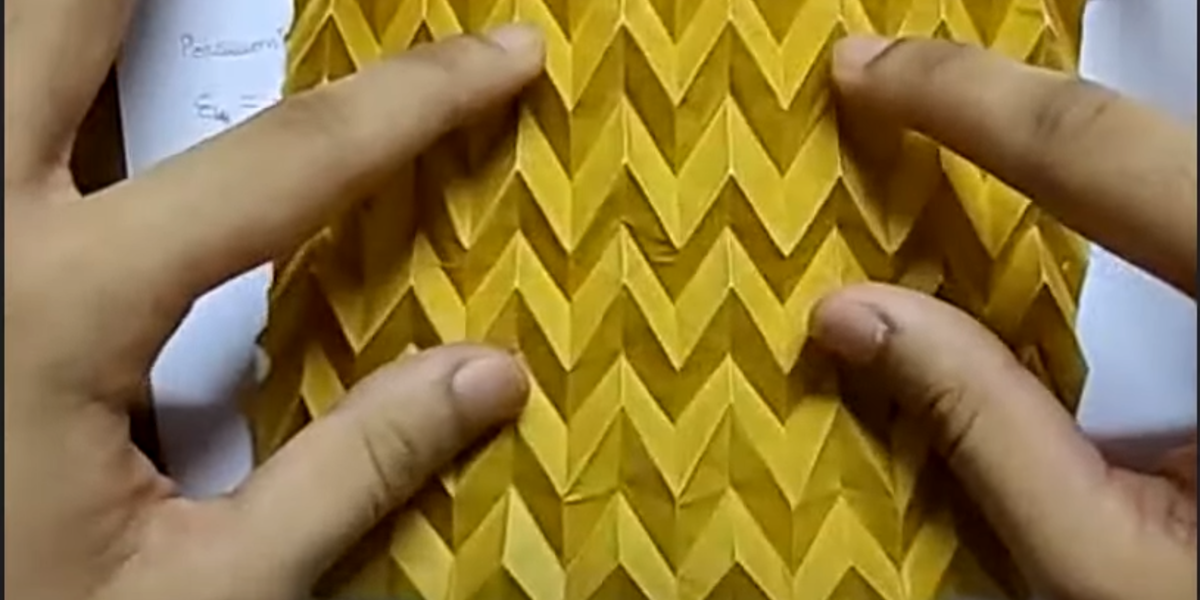
In the first half of his workshop, Naman Pushp walks you through some of the important first concepts in mechanical engineering — how to think about the forces in the world that act on physical objects. And he brings along a great range of home-built Jugaad props that include a gravity-defying tensegrity string sculpture and some fancy origami that help hammer the topics home.

In the second half of the workshop, Naman takes these concepts into computer simulation, and gives us good insight into the way that finite-element analysis simulation packages model these same forces on tiny chunks of your project’s geometry to see if it’ll hold up under real world load. The software he uses isn’t free by any definition — it’s not even cheap unless you have a student license — but it’s nonetheless illuminating to watch him work through the flow of roughly designing an object, putting simulated stresses and strains on it, and interpreting the results. If you’ve never used FEA tools before, or are looking for a compressed introduction to first-semester mechanical engineering, this talk might be right up your alley. Continue reading “Remoticon Video: The Mechanics Of Finite Element Analysis”

Remoticon Video: From Zero To ASIC; How To Design In Silicon

Designing your own integrated circuits as a one-person operation from your home workshop sounds like science fiction. But 20 years ago, so did rolling your own circuit boards to host a 600 MHz microcontroller with firmware you wrote yourself. Turns out silicon design isn’t nearly as out of reach as it used to be and Matt Venn shows us the ropes in his Zero to ASIC workshop.

Held during the 2020 Hackaday Remoticon, this is a guided tour of the tools used in the Skywater PDK — the Process Design Kit that is an open-source ASIC toolkit produced in a partnership between Google and SkyWater Technology. We covered the news when first announced back in June, but this the most comprehensive look we’ve seen into the actual design process.

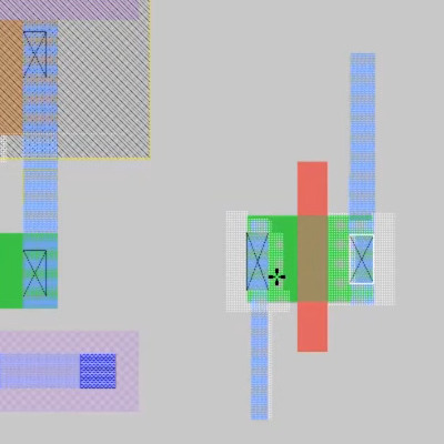
Drawing N-channel MOSFET in silicon

Matt builds up the demo starting from the very simple design of an N-channel MOSFET with click-and-drag tools similar to graphics editing software. The good news it that although you can draw your own structures like this, for digital designs you won’t have to. A wide variety of IP has been contributed to the open source project allowing basic building blocks to be pulled in using HDL. However, the power of drawing structures will certainly be the playground for those needing analog design as part of their projects.

As with EDA software used for circuit boards, the PDK includes design rule checks to ensure you aren’t violating the limits of the 130 nm chip fab. There’s some other black magic in there too, as Matt specifically mentions an antenna rules check to safeguard your design from being fried by induced current on “large” (microscopically so) metalized runs during the fabrication process.

Part of a massive logic flow chart for an IC counter design

The current workflow involves grinding through a large number of configuration files, something Matt admits took him a long time to wrap his head around. However, what’s available for proofing your design is very impressing. He demonstrates SPICE simulation to calculate timings, and shows numerous examples of verification drawings generated by the compilation process, either in the form of seeing the structures as they will be laid out, or as logical flow charts. This is crucial as a single run will take 2-3 months to come back from fab — you want to get things right before buttoning up the project. Incidentally, that’s know as “tapeout”, a term you’ve likely heard before and he says it comes from reels of magnetic tape containing the design being removed from the computer and sent to production. Who knew? (This tidbit in strikethrough appears to be incorrect).

But wait, there’s more to this than just designing the things. Part of the intrigue of the Skywater-PDK project is that Google bought into covering a group run about once per quarter so that open-source designs can be ganged onto a multi-project wafer free of charge to the people submitting them. That’s pretty awesome and we’re giddy to hear news of people getting their wafer-level chip scale devices — also known as flip chips — back for testing. Matt is planning a more in-depth paid course on the topic. For now, get a taste of what’s involved from this excellent workshop found after the break.

Continue reading “Remoticon Video: From Zero To ASIC; How To Design In Silicon”

Remoticon Video: KiCad To Blender PCB Renders

We seem to want our PCB design software to do everything these days, and it almost delivers. You can not only lay it all out, check electrical and design rules, and even spit out a bill of materials, but many PCB tools produce 3D models that are good enough to check parts clearance or are useful in designing enclosures. But when it comes to producing photorealistic output, whether for advertising or just for eye-candy, you might want to turn to 3D design tools.

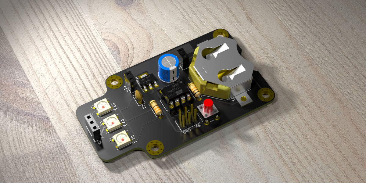
In this workshop, Anool Mahidharia takes the output of KiCad’s VRML export, gets it rendering in Blender, and then starts tweaking the result until you’re almost not sure if it’s the real thing or a 3D model. He starts off with a board in KiCad, included in the project’s GitHub repo, and you can follow along through the basic import, or go all the way to copying the graphics off the top of an ATtiny85 and making sure that the insides of the through-plated holes match the tops.

If you don’t know Blender, maybe you don’t know how comprehensive a 3D modelling and animation tool it is. And with the incredible power comes a notoriously steep learning curve up a high mountain. Anool doesn’t even try to turn you into a Blender expert, but focuses on the tweaks and tricks that you’ll need to make good looking PCB renders. You’ll find general purpose Blender tutorials everywhere on the net, but if you want something PCB-specific, you’ve come to the right place.

Continue reading “Remoticon Video: KiCad To Blender PCB Renders”

Remoticon Video: Making Glowy Origami With Charlyn Gonda

Hacking is about pushing the envelope to discover new and clever ways to use things in ways their original designers never envisioned. [Charlyn Gonda]’s Hackaday Remoticon workshop “Making Glowly Origami” was exactly that; a combination of the art of origami with the one of LEDs. Check out the full course embedded below, and read on for a summary of what you’ll find. Continue reading “Remoticon Video: Making Glowy Origami With Charlyn Gonda”

Remoticon Video: How To 3D Print Onto Fabric With Billie Ruben

We’re impressed to see the continued flow of new and interesting ways to utilize 3D printing despite its years in the hacker limelight. At the 2020 Hackaday Remoticon [Billie Ruben] came to us from across the sea to demonstrate how to use 3D printing and fabric, or other flexible materials, to fabricate new and interesting creations. Check out her workshop below, and read on for more detail about what you’ll find.

The workshop is divided into two parts, a hands-on portion where participants execute a fabric print at home on their own printer, and a lecture while the printers whirr away describing ways this technique can be used to produce strong, flexible structures.

The technique described in the hands on portion can be clumsily summarized as “print a few layers, add the flexible material, then resume the printing process”. Of course the actual explanation and discussion of how to know when to insert the material, configure your slicer, and select material is significantly more complex! For the entire process make sure to follow along with [Billie]’s clear instructions in the video.

The lecture portion of the workshop was a whirlwind tour of the ways which embedded materials can be used to enhance your prints. The most glamourous examples might be printing scales, spikes, and other accoutrement for cosplay, but beyond that it has a variety of other uses both practical and fashionable. Embedded fabric can add composite strength to large structural elements, durable flexibility to a living hinge, or a substrate for new kinds of jewelry. [Billie] has deep experience in this realm and she brings it to bear in a comprehensive exposition of the possibilities. We’re looking forward to seeing a flurry of new composite prints!