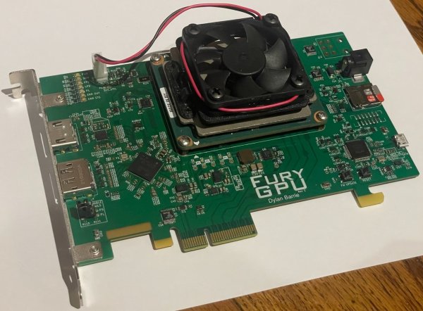
Have you ever wondered how a GPU works? Even better, have you ever wanted to make one? [Dylan] certainly did, because he made FuryGPU — a fully custom graphics card capable of playing Quake at over 30 frames per second.
As you might have guessed, FuryGPU isn’t in the same league as modern graphics card — those are made of thousands of cores specialized in math, which are then programmed with whatever shaders you want. FuryGPU is a more “traditional” GPU, it has dedicated hardware for all the functions the GPU needs to perform and doesn’t support “shader code” in the same way an AMD or NVIDIA GPU does. According to [Dylan], the hardest part of the whole thing was writing Windows drivers for it.
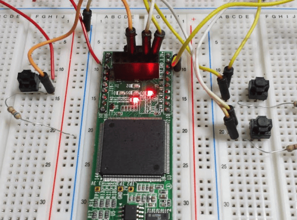
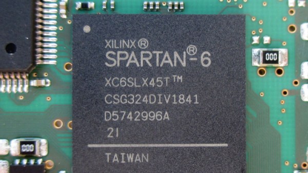
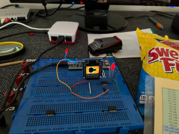
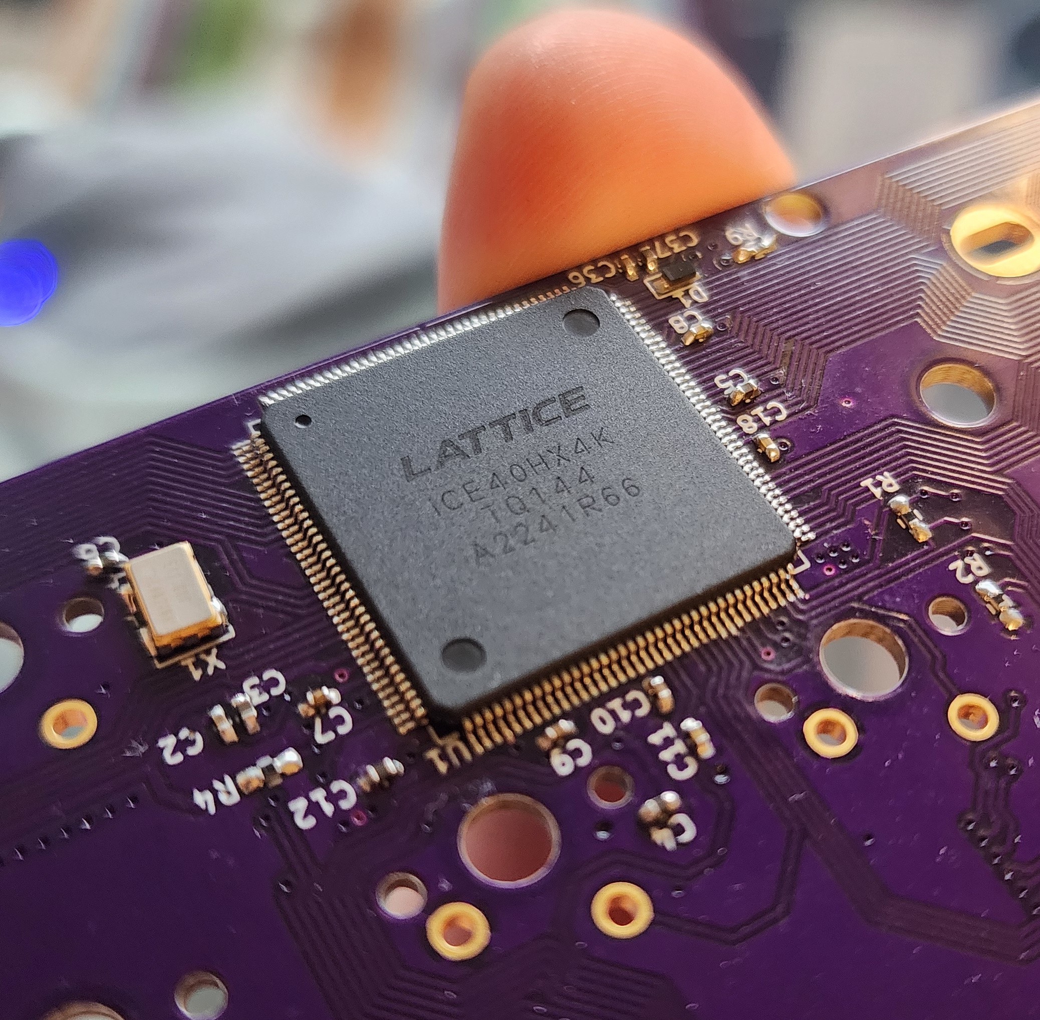
On his blog, [Dylan] tells us all about how he went from the obligatory [Ben Eater] breadboard CPU to playing with FPGAs to even larger FPGAs to bear the weight of this mighty GPU. While this project isn’t exactly revolutionary in the GPU world, it certainly is impressive and we impatiently wait to see what comes next.