Today’s supply chain issues can make it hard to buy microcontrollers, or really any kind of semiconductor. But for those keeping retrocomputers alive, this problem has always existed: ancient components might have been out of production for decades, with a dwindling supply of second-hand parts or “new old stock” as the only option. If a rare CPU breaks, you might have no option but to replace the entire computer.
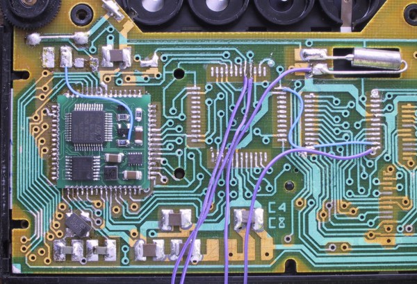
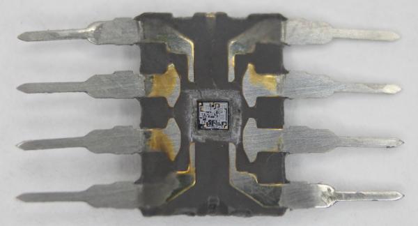
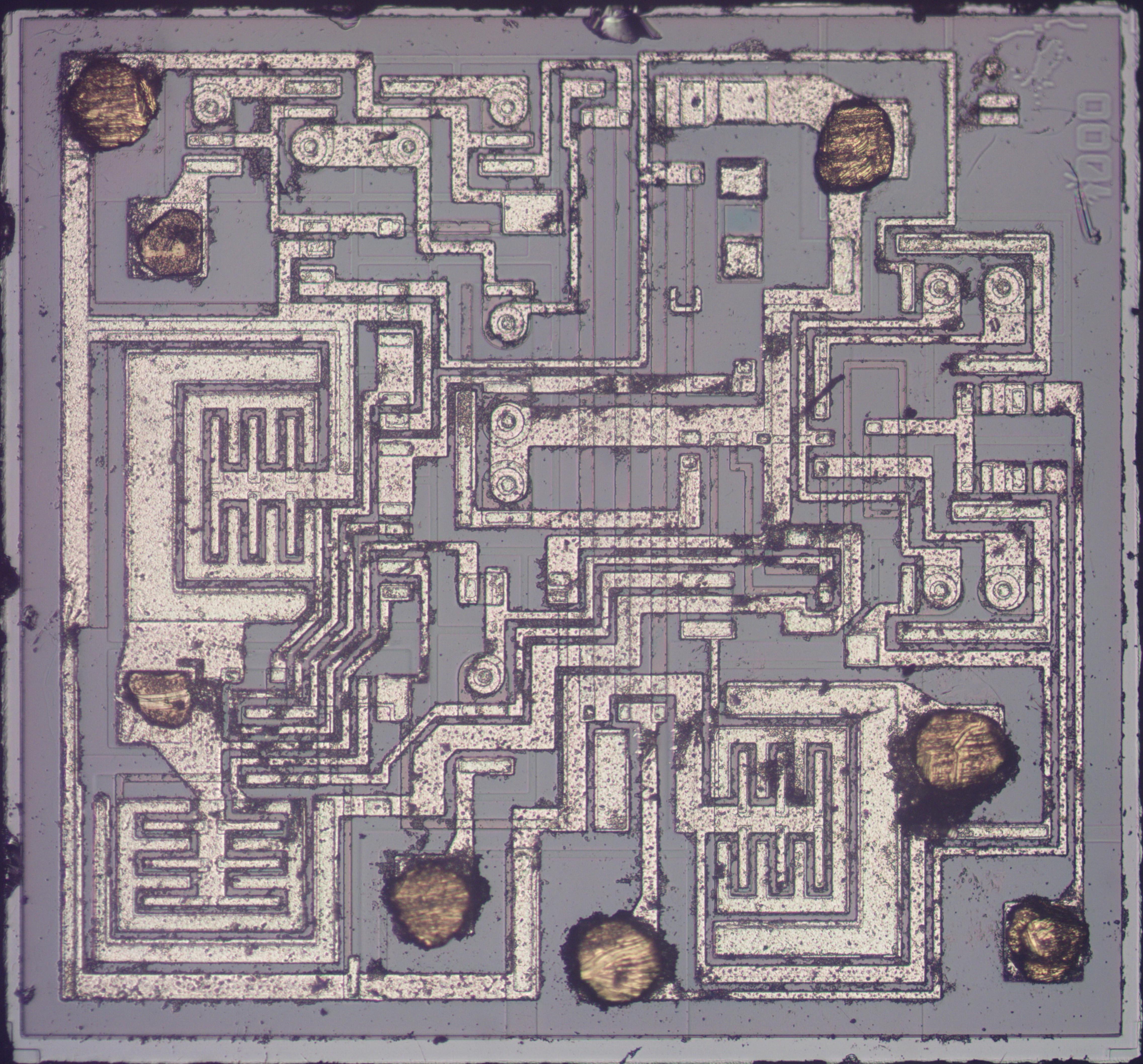
[Piotr Patek] ran into this issue when he obtained an Elektronika MK-85 programmable calculator with a broken CPU. Unable to find a replacement, he decided instead to build a pin-compatible CPU unit based on an STM32 microcontroller. Of course no modern CPU is pin-compatible with a Soviet design from the 1980s, so [Piotr] had to design a small interposer PCB to match the original pinout. This also gave him enough space to add an efficient DC/DC converter chip that generates the 2.5 V supply for the STM32.
As for the software, [Piotr] managed to port the original BASIC interpreter, which was written in PDP-11 assembly, to a modern equivalent written in C. While he was at it, he fixed a few bugs that had been sitting there for about 35 years. The updated CPU also allows the MK-85 to run circles around its contemporary siblings: [Piotr] timed it to be about thirty times faster than the original chip, while using a comparable amount of power.
If you also happen to have an MK-85 with a dodgy CPU, you’ll be pleased to find that the schematics and source code to [Piotr]’s modification are all available on his blog. This is probably the first calculator CPU update we’ve seen, although we’ve featured other ancient calculators updated with new firmware, and some completely new calculator designs based on classic hardware.
Thanks for the tip, [cmholm]!