Home machinists can often find great deals on used industrial equipment, and many a South Bend lathe or Bridgeport milling machine has followed someone home. Then comes the moment to plug it in, and the new owner discovers that the three-phase plug needed to power the new beast is nowhere to be found in the shop. Thus commences the weeping and the gnashing of teeth.
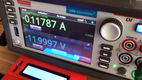
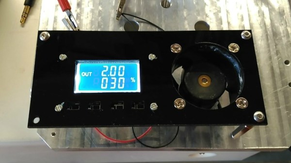
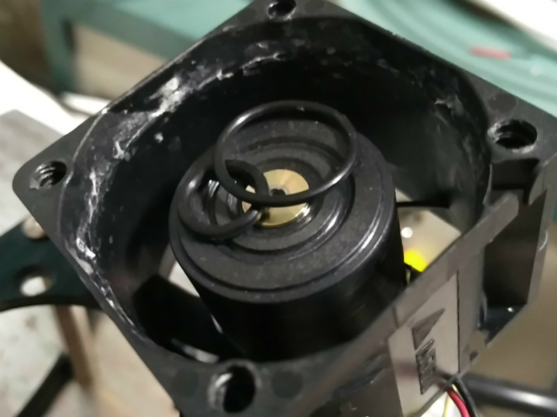
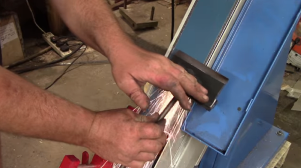
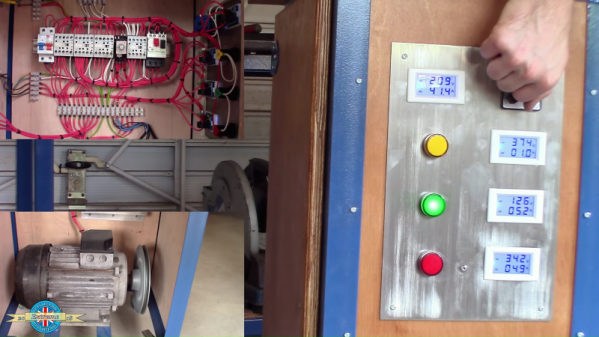
Luckily, [Handmade Extreme] is ahead of the curve in terms of shop power, and built a rotary phase converter to power his machines. Industry generally runs on three-phase AC systems, mainly because three-phase electric motors are so much more efficient and compact than the equivalent single-phase motor. But residential electrical service is either split-phase or, in the UK where [Handmade Extreme] is based, single phase. A rotary phase converter is an electromechanical device that can generate the missing phases – in essence a three-phase motor that can run on one winding and generate the missing phases across the other windings. It needs some supporting control circuitry to do so, such as timers and contactors to switch the winding connections once the motor starts, plus capacitors for motor starting and for balancing the voltage across the phases. The control gear is DIN-rail mounted and neatly wired to a smart-looking control panel. Everything is housed in a sturdy enclosure that’s big enough to serve as a mobile tool cart. It’s a really nice job – watch the whole build in the video below.
If you’re interested in power distribution, we’ve got a primer that covers the basics. And if you’re in the market for machine tools, [Quinn]’s machine tool buyer’s guide will let you decide if a three-phase machine is worth the extra effort.
Continue reading “Rolling Out A Slick Rotary Phase Converter”