So you’ve finished your project. You’ve got a wonderful circuit, a beautiful PCB, and everything works perfectly. You’re done right? Well, maybe not. Sure, a bare PCB might be fine for a dev board, but what if you have a LCD to mount, a knob that needs turning, and buttons that need pressing. Yeah, that potentiometer hanging off the board by a few wires isn’t so pretty, is it? So it’s time for a case. Yuck. We all hate modifying cases.
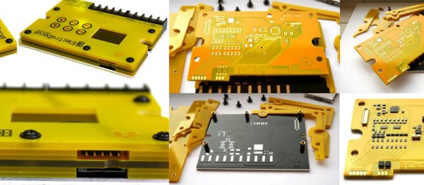
[Electrodacus] came up with a clever solution in the form of stacking PCBs to form a case. In his project, he actually has the circuitry spread across 3 PCBs, and uses surface mount connectors to connect them in a stack. Along the edges are specifically shaped PCBs to complete the enclosure. This technique could be used with only one PCB containing all the circuitry, and the others acting as the case sides and top.
In this solar battery management project, the base layer has most of the power circuitry. This layer uses an aluminum metal core PCB for heat dissipation. The center layer is home for the micro controller and supporting components. And the top layer is the “front panel” with capacitive touch buttons and a cut out for a LCD. The top layer silk screen contains the logo, button markings, and the pin out of all the connectors.
If you hate drilling and filling cases (as much as we do), this technique might be right for your next project.
[via EEVBlog Forums]