FPGA Computer Covers A To Z

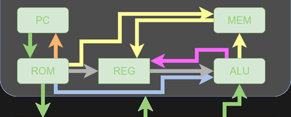
[F4HDK] calls his new computer A2Z because he built everything from scratch (literally, from A to Z). Well, strictly speaking, he did start with an FPGA, but you have to have some foundation. The core CPU is a 16-bit RISC processor with a 24-bit address bus and a 128-word cache. The computer sports 2 megabytes of RAM, a boot ROM, a VGA port and keyboard, and some other useful I/O. The CPU development uses Verilog.

Software-wise, the computer has a simple operating system, a filesystem, and basic programs like a text editor and an image viewer. Development software includes an assembler and a compiler for a BASIC-like language that resides on the PC. You can also run an emulator to experiment with A2Z without hardware. You can see a “car game” running on A2Z in the video below. You can also see videos of some other applications.

Continue reading “FPGA Computer Covers A To Z”

Make Mulled Wine With A Processor Heatsink!

Now, over the holiday season there seems to be a predilection towards making merry and bright. As many an engineer and otherwise are sure to note, fine alcohols will facilitate this process. One such warm holiday beverage is mulled wine; there are many traditions on how to make it, but a singular approach to preparing the beverage would be to re-purpose an old PC and a CPU liquid cooling unit into a mulled wine heating station.

Four years ago, [Adam] found himself staring at a pile of mostly obsolete PCs in his IT office and pondering how they could be better used. He selected one that used a power-hungry Pentium 4 — for its high heat output — strapped a liquid cooling block to the CPU and pumped it full of the holiday drink. It takes a few hours to heat three liters of wine up to an ideal 60 Celsius, but that’s just in time for lunch! The Christmastime aroma wafting through the office is nice too.

Continue reading “Make Mulled Wine With A Processor Heatsink!”

One Bit, One Instruction Discrete CPU

There is a certain benefit to being an early adopter. If you were around when Unix or MSDOS had a handful of commands, it wasn’t hard to learn. Then you learn new things as they come along. If you started learning Linux or Windows today, there’s a huge number of details you have to tackle. You have the same problem trying to learn CPU design. Grappling with the design of a 16-bit CPU with a straightforward data path is hard enough. Throw in modern superscalar execution, pipelining, multiple levels of microcode, speculative execution, and all the other features modern processors have and you’ll quickly find yourself lost in the details.

[Michai Ramakers] wanted to build an educational CPU and he took a novel approach. The transistor CPU uses only one instruction and operates on one bit at a time. Naturally, this leads to a small data path, which is a good thing if you’re only using discrete transistors. His website is a ground-up tutorial in building and using the tiny computer.

Continue reading “One Bit, One Instruction Discrete CPU”

1MHz, 2 Boards, 4 Bits And A Homebrew CPU

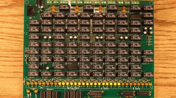
[Agp.cooper] saw a vintage 4Kx4 bit RAM chip and decided that it needed a CPU design to match. The TTL design fits on two boards and has a functional front panel.

This custom CPU project has a few interesting bits worth noting. First, it is small enough that you can wrap your head around it pretty easily. And [Agp.cooper] gives  a good account of the instructions set architecture choices he considered and why he settled on the final design.

Continue reading “1MHz, 2 Boards, 4 Bits And A Homebrew CPU”

Weird CPU

How many instructions does [agp.cooper’s] computer have? Just one. How many strip boards does it use? Apparently, 41 five 41-track boards. While being one shy from the answer to life, it is still a lot of boards for a single instruction. The high board count is due to the use of 1970’s vintage ICs including TTL parts, 2114 RAM chips, and 74S571 PROMs.

There are several different architectures for single instruction computers and [agp’s] uses what is technically at TTA (transfer-triggered architecture). That is, the one instruction is a move and the destination or source of the move determines the operation. For example, the Wierd CPU (that’s the name of it) has a P and Q register. If you load those registers and then the ADD register will contain the sum of the two numbers.

Continue reading “Weird CPU”

1000 CPUs On A Chip

Often, CPUs that work together operate on SIMD (Single Instruction Multiple Data) or MISD (Multiple Instruction Single Data), part of Flynn’s taxonomy. For example, your video card probably has the ability to apply a single operation (an instruction) to lots of pixels simultaneously (multiple data). Researchers at the University of California–Davis recently constructed a single chip with 1,000 independently programmable processors onboard. The device is energy efficient and can compute up to 1.78 trillion instructions per second.

The KiloCore chip (not to be confused with the 2006 Rapport chip of the same name) has 621 million transistors and uses special techniques to be energy efficient, an important design feature when dealing with so many CPUs. Each processor operates at 1.78 GHz or less and can shut itself down when not needed. The team reports that even when computing 115 billion instructions per second, the device only consumes about 700 milliwatts.

Unlike some multicore designs that use a shared memory area to communicate between processors, the KiloCore allows processors to directly communicate. If you are just a diehard Arduino user, maybe you could scale up this design. Or, if you want to make use of the unused power in your video card under Linux, you can always try to bring KGPU up to date.

A Dis-Integrated 6502

The 6502 is the classic CPU. This chip is found in the original Apple, Apple II, PET, Commodore 64, BBC Micro, Atari 2600, and 800, the original Nintendo Entertainment System, Tamagotchis, and Bender Bending Rodriguez. This was the chip that started the microcomputer revolution, and holds a special place in the heart of every nerd and technophile. The 6502 is also possibly the most studied processor, with die shots of polysilicon and metal found in VLSI textbooks and numerous simulators available online.

The only thing we haven’t seen, until now, is a version of the 6502 built out of discrete transistors. That’s what [Eric Schlaepfer] has been working on over the past year. It’s huge – 12 inches by 15 inches – has over four thousand individual components, and so far, this thing works. It’s not completely tested, but the preliminary results look good.

The MOnSter 6502 began as a thought experiment between [Eric] and [Windell Oskay], the guy behind Evil Mad Scientist and creator of the discrete 555 and dis-integrated 741 kits. After realizing that a few thousand transistors could fit on a single panel, [Eric] grabbed the netlist of the 6502 from Visual6502.org. With the help of several scripts, and placing 4,304 components into a board design, the 6502 was made dis-integrated. If you’re building a CPU made out of discrete components, it only makes sense to add a bunch of LEDs, so [Eric] threw a few of these on the data and address lines.

This is the NMOS version of the 6502, not the later, improved CMOS version. As such, this version of the 6502 doesn’t have all the instructions some programs would expect. The NMOS version is slower, more prone to noise, and is not a static CPU.

So far, the CPU is not completely tested and [eric] doesn’t expect it to run faster than a few hundred kilohertz, anyway. That means this gigantic CPU can’t be dropped into an Apple II or commodore; these computers need a CPU to run at a specific speed. It will, however, work in a custom development board.

Will the gigantic 6502 ever be for sale? That’s undetermined, but given the interest this project will receive it’s a foregone conclusion.

Correction: [Eric] designed the 555 and 741 kits