Even with ten fingers to work with, math can be hard. Microprocessors, with the silicon equivalent of just two fingers, can have an even harder time with calculations, often taking multiple machine cycles to figure out something as simple as pi. And so 40 years ago, Intel decided to give its fledgling microprocessors a break by introducing the 8087 floating-point coprocessor.
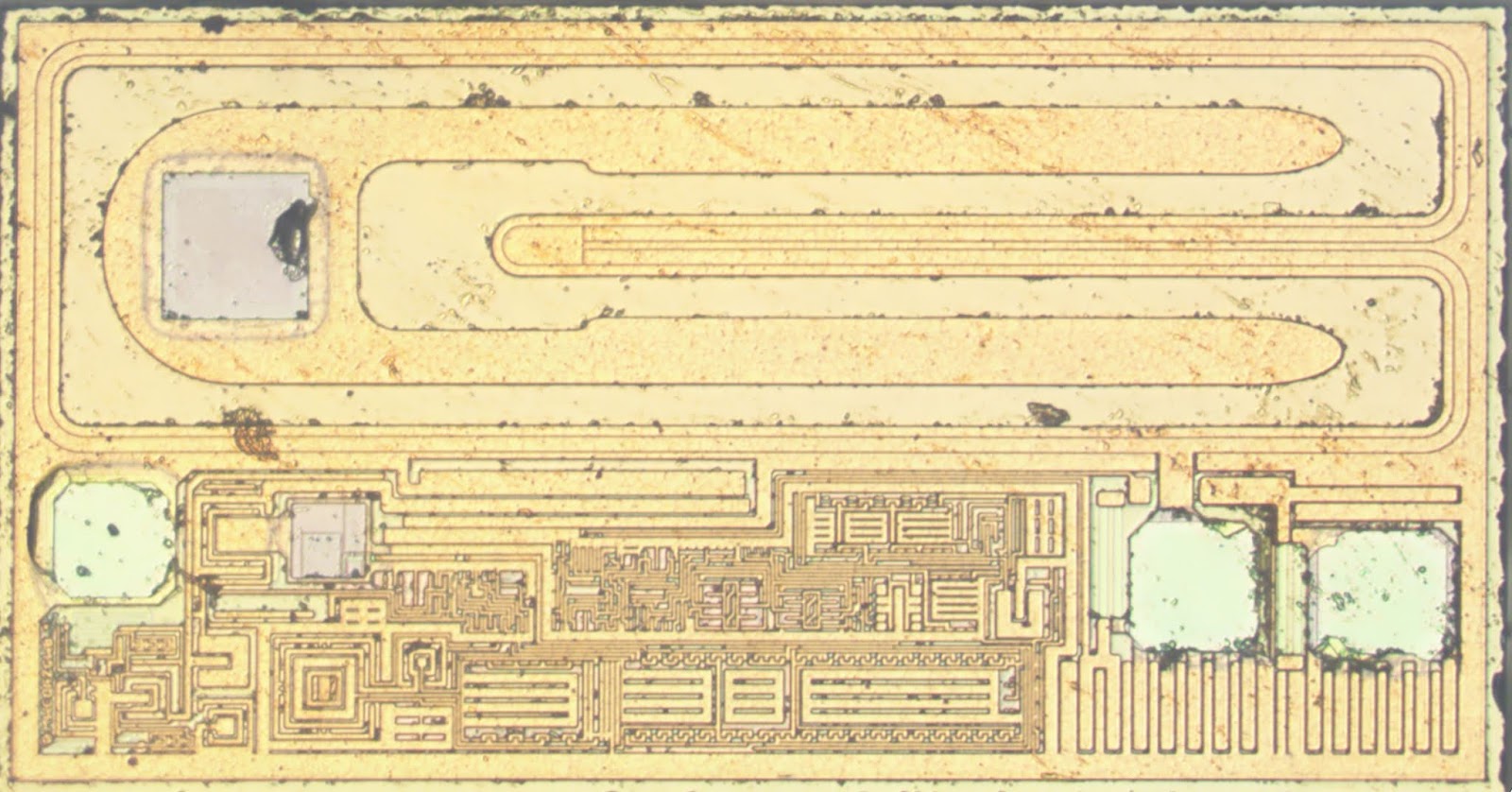
If you’ve ever wondered what was going on inside the 8087, wonder no more. [Ken Shirriff] has decapped an 8087 to reveal its inner structure, which turns out to be closely related to its function. After a quick tour of the general layout of the die, including locating the microcode engine and ROM, and a quick review of the NMOS architecture of the four-decade-old technology, [Ken] dug into the meat of the coprocessor and the reason it could speed up certain floating-point calculations by up to 100-fold. A generous portion of the complex die is devoted to a ROM that does nothing but store constants needed for its calculation algorithms. By carefully examining the pattern of NMOS transistors in the ROM area and making some educated guesses, he was able to see the binary representation of constants such as pi and the square root of two. There’s also an extensive series of arctangent and log2 constants, used for the CORDIC algorithm, which reduces otherwise complex transcendental calculations to a few quick and easy bitwise shifts and adds.
[Ken] has popped the hood on a lot of chips before, finding butterflies in an op-amp and reverse-engineering a Sinclair scientific calculator. But there’s something about seeing constants hard-coded in silicon that really fascinates us.