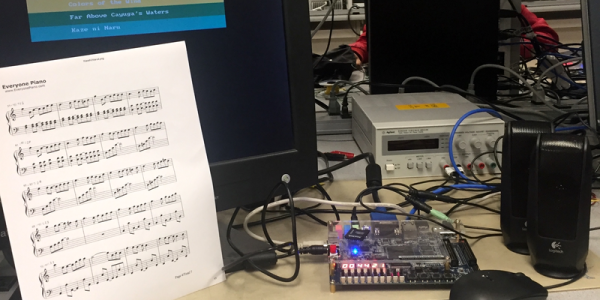
The human auditory system is a complex and wonderful thing. One of its most useful features is the ability to estimate the range and direction of sound sources – think of the way people instinctively turn when hearing a sudden loud noise. A team of students have leveraged this innate ability to produce a game of tag based around nothing but sound.
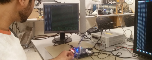
The game runs on two FPGAs, which handle the processing and communication required. The chaser is given a screen upon which they can see their own location and that of their prey. The target has no vision at all, and must rely on the sounds in their stereo headphones to detect the location of the chaser and evade them as long as possible.
The project documentation goes into great detail about the specifics of the implementation. The game relies on the use of the Head Related Transfer Function – a function related to how the ear picks up sounds relative to their position. This allows the FPGA to simulate the chaser’s footsteps, and feed the audio to the target who perceives the chaser’s position purely by sound.
It’s a great example of a gameplay mechanic that we’d love to see developed further. The concept of trying to find one’s way around by hearing alone is one which we think holds a lot of promise.
With plenty of processing power under the hood, FPGAs are a great choice for complex audio projects. A great project to try might be decoding MP3s.