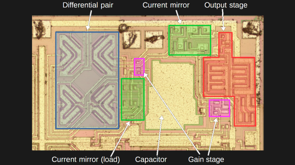
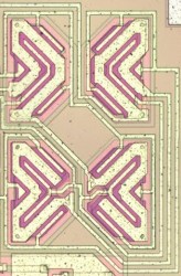
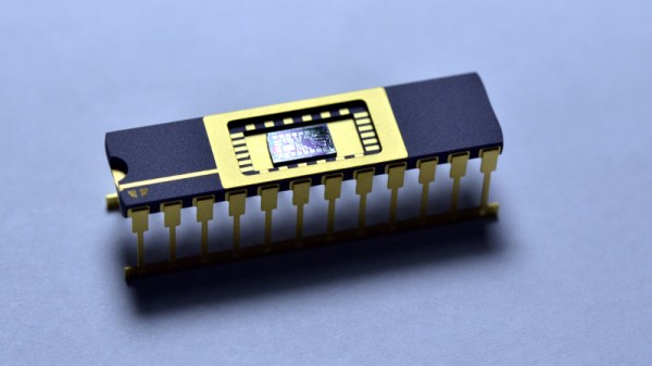
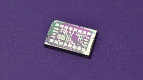
TL084 die blocks

Ken Shirriff Found Butterflies In His Op-Amp

In 1976, Texas Instruments came out with the TL084, a four JFET op-amp IC each with similar circuitry to Fairchild’s very popular single op-amp 741. But even though the 741 has been covered in detailed, when [Ken Shirriff] focused his microscope on a TL084, he found some very interesting things.

JFETs on the TL084 op-amp

To avoid using acid to get at the die, he instead found a ceramic packaged TL084 and pried off the cover. The first things he saw were four stabilizing capacitors, by far the largest structures on the die and visible to the naked eye.

When he peered into his microscope he next saw butterfly shapes which turned out to be pairs of input JFETs. The wide strips are the gates and the narrower strip surrounded by each gate is the source. The drain is the narrow strip surrounding each gate. Why arrange four JFETs like this? It’s possible to have temperature gradients in the IC, one side being hotter than the other. These gradients can affect the JFET’s characteristics, unbalancing the inputs. Look closely at the way the JFETs are connected and you’ll see that the top-left one is connected to the bottom-right one, and similarly for the other two. This diagonal cross-connecting cancels out any negative effects.

[Ken’s] analysis in his article doesn’t stop there though. Not only does he talk more about these JFETs but he goes over the rest of the die too. It’s well worth the read, as is his write-up about the 741 which we’ve also covered.

More Details On That First Home-Made Lithographically Produced IC

A few days ago we brought you news of [Sam Zeloof]’s amazing achievement, of creating the first home-made lithographically produced integrated circuit. It was a modest enough design in a simple pair of differential amplifiers and all we had to go on was a Twitter announcement, but it promised a more complete write-up to follow. We’re pleased to note that the write-up has arrived, and we can have a look at some of the details of just how he managed to produce an IC in his garage. He’s even given it a part number, the Zeloof Z1.

For ease of manufacture he’s opted for a PMOS process, and he is using four masks which he lists as the active/doped area, gate oxide, contact window, and top metal. He takes us through 66 different processes that he performs over the twelve hours of a full production run, with comprehensive descriptions that make for a fascinating run-down of semiconductor manufacture for those of us who will never build a chip of our own but are still interested to learn how it is done. The chip’s oblong dimensions are dictated by the constraints of an off-the-shelf Kyocera ceramic chip carrier, though without a wire bonding machine he’s unable to do any more than test it with probes.

You can read our reporting of his first announcement, but don’t go away thinking that will be all. We’re certain [Sam] will be back with more devices, and can’t wait to see the Z2.

First Lithographically Produced Home Made IC Announced

It is now six decades since the first prototypes of practical integrated circuits were produced. We are used to other technological inventions from the 1950s having passed down the food chain to the point at which they no longer require the budget of a huge company or a national government to achieve, but somehow producing an integrated circuit has remained out of reach. It’s the preserve of the Big Boys, move on, there’s nothing to see here.

Happily for us there exists a dedicated band of experimenters keen to break that six-decade dearth of home-made ICs. And now one of them, [Sam Zeloof], has made an announcement on Twitter that he has succeeded in making a dual differential amplifier IC using a fully lithographic process in his lab. We’ve seen [Jeri Ellsworth] create transistors and integrated circuits a few years ago and he is at pains to credit her work, but her interconnects were not created lithographically, instead being created with conductive epoxy.

For now, all we have is a Twitter announcement, a promise of a write-up to come, and full details of the lead-up to this momentous event on [Sam]’s blog. He describes both UV lithography using a converted DLP projector and electron beam lithography using his electron microscope, as well as sputtering to deposit aluminium for on-chip interconnects. We’ve had an eye on his work for a while, though his progress has been impressively quick given that he only started amassing everything in 2016. We look forward to greater things from this particular garage.

Blast From The Past With Space Station PROM Reader

The Ursa Major Space Station SST282 is a dinosaur of a digital reverb.  Okay, so maybe 1978 isn’t ancient yet, but it is getting to the point where one has to worry about the possibility of component failure.  At least that’s what [Obsoletetechnology] thought when they created a backup of its memory contents.

As can be seen from some of Hackaday’s previous articles, a part does not have to be an older one to fail.  However, there is no such thing as being too paranoid when it comes to older parts reaching their lifetime.  Especially when there is valuable memory involved.  Each bit of PROM memory is locked by a fuse on its location grid to store permanent data.  To be able to read this and collect the respective data, a Raspberry Pi 3 PROM reader was created.

The SST282 uses 3 TTL-level 74xx series Schottky PROM memories on board that hold RAM lookup tables.  In the case that these failed, all of the subsequent information would be lost since there are no surviving memory dumps online.  Fortunately we are interested only in gathering their contents, so the PROM reader schematic is fairly rudimentary.  The chip’s address and data buses connect to a Pi’s GPIO header, and the only other thing to note is a 74LS541 TTL level shifter that converts the Pi’s 3.3V output to the PROM’s 5V TTL level.

Continue reading “Blast From The Past With Space Station PROM Reader”

Get Down To The Die Level With This Internal Chip Repair

Usually, repairing a device entails replacing a defective IC with a new one. But if you’ve got young eyes and haven’t had caffeine in a week, you can also repair a defective chip package rather than replace it.

There’s no description of the incident that resulted in the pins of the QFP chip being ablated, but it looks like a physical insult like a tool dropped on the pins. [rasminoj]’s repair consisted of carefully grinding away the epoxy cap to expose the internal traces leading away from the die and soldering a flexible cable with the same pitch between the die and the PCB pads.

This isn’t just about [rasminoj]’s next-level soldering skills, although we’ll admit you’ve got to be pretty handy with a Hakko to get the results shown here. What we’re impressed with is the wherewithal to attempt a repair that requires digging into the chip casing in the first place. Most service techs would order a new board, or at best solder in a new chip. But given that the chip sports a Fanuc logo, our bet is that it’s a custom chip that would be unreasonably expensive to replace, if it’s even still in production. Where there’s a skill, there’s a way.

Need more die-level repairs? Check out this iPhone CPU repair, or this repair on a laser-decapped chip.

[via r/electronics]

Popping The Top Of A Ceramic IC

If you’ve ever wanted to open up an IC to see what’s inside it, you have a few options. The ceramic packages with a metal lid will succumb to a hobby knife. That’s easy. The common epoxy packages are harder, and usually require a mix of mechanical milling and the use of an acid (like fuming nitric, for example). [Robert Baruch] wanted to open a fully ceramic package so he used the “cooler” part of a MAP gas torch. If you like seeing things get hot in an open flame, you might enjoy the video below.

Spoiler alert: [Robert] found out the hard way that dropping the hot part isn’t a great idea. Also, we are not sure what the heat does if you want to do more than just inspect the die. It would be interesting to measure a junction on the die during the process to see how much heat actually goes to the device.

Continue reading “Popping The Top Of A Ceramic IC”

8008 Exposed

[Ken Shirriff] is no stranger to Hackaday. His latest blog post is just the kind of thing we expect from him: a tear down of the venerable 8008 CPU. We suspect [Ken’s] earlier post on early CPUs pointed out the lack of a good 8008 die photo. Of course, he wasn’t satisfied to just snap the picture. He also does an analysis of the different constructs on the die.

Ever wonder why the 8008 ALU is laid out in a triangle shape? In all fairness, you probably haven’t, but you might after you look at the photomicrograph of the die. [Ken] explains why.

Continue reading “8008 Exposed”