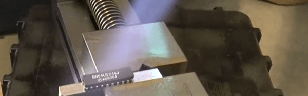
If you’ve ever wanted to open up an IC to see what’s inside it, you have a few options. The ceramic packages with a metal lid will succumb to a hobby knife. That’s easy. The common epoxy packages are harder, and usually require a mix of mechanical milling and the use of an acid (like fuming nitric, for example). [Robert Baruch] wanted to open a fully ceramic package so he used the “cooler” part of a MAP gas torch. If you like seeing things get hot in an open flame, you might enjoy the video below.
Spoiler alert: [Robert] found out the hard way that dropping the hot part isn’t a great idea. Also, we are not sure what the heat does if you want to do more than just inspect the die. It would be interesting to measure a junction on the die during the process to see how much heat actually goes to the device.
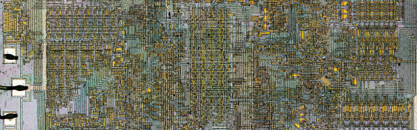
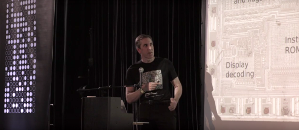
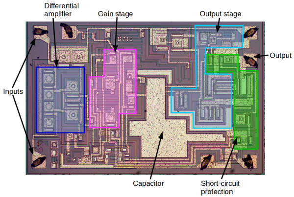
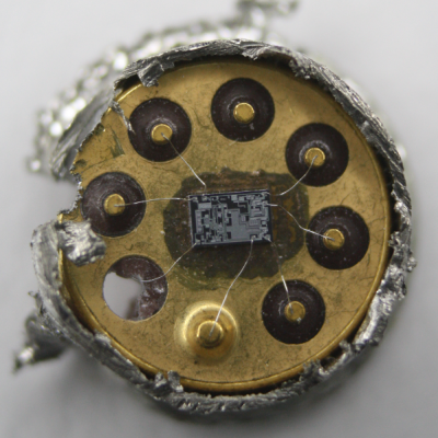 Rather than risk the boiling acid method commonly used to decap epoxy-potted ICs, [Ken] wisely chose a TO-99 can format to attack with a hacksaw. With the die laid bare for his microscope, he was able to locate all the major components and show how each is implemented in silicon. Particularly fascinating is the difference between the construction of NPN and PNP transistors, and the concept of “current mirrors” as constant current sources. And he even whipped up a handy interactive chip viewer – click on something in the die image and find out which component it is on the 741 schematic. Very nice.