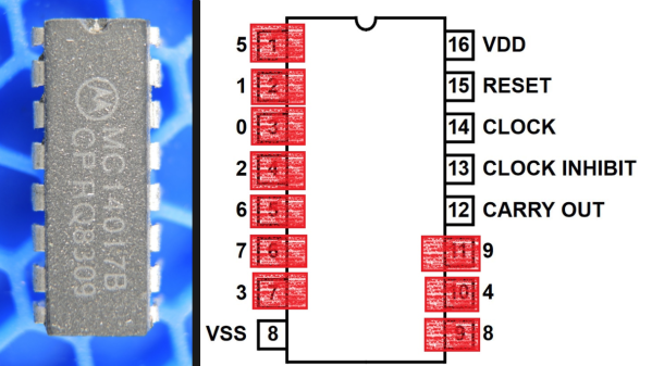
If you’ve ever handled a chip with a really strange or highly inconvenient pinout and suspected that the reason had something to do with the inner workings, you may be interested to see [electronupdate]’s analysis of why the 4017 Decade Counter IC has such a weirdly nonintuitive pinout. It peeks into an IC design dating from the 1970s to see an example of the kind of design issues that can affect physical layout.
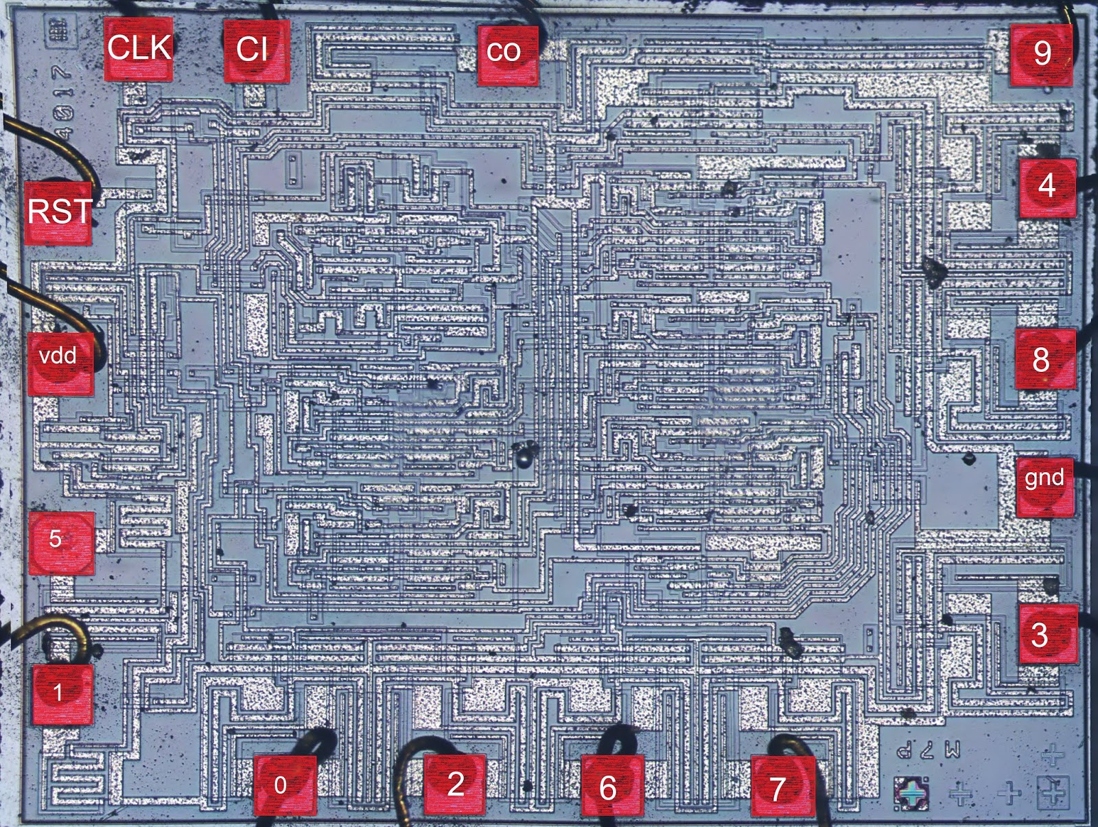
In the case of the 4017, once decapped and the inner workings exposed, things became more clear. Inside the chip are a bunch of flip-flops and NAND gates, laid out in a single layer. Some of the outputs (outputs 5 and 1 for example, physically on pins 1 and 2 respectively) share the same flip-flop.
The original design placed the elements in a way that made the most logical sense for routing and layout, which resulted in nice and tidy inner workings but an apparently illogical pinout. A lot of this is probably feeling familiar to anyone who has designed and routed a single-layer PCB, where being limited to one layer makes it important to get the most connections as directly near one another as possible.
Chip design has of course come a long way since the 70s, but there is forever some level of trade-off to be made between outward tidiness and inner design harmony. The next time you’re looking at a part with an apparently illogical pinout, there’s a fair chance it makes far more sense on the inside.
We get it, press releases are full of hyperbole. Cerebras recently announced they’ve built the largest chip ever. The chip has 400,000 cores and contains 1.2 trillion transistors on a die over 46,000 square mm in area. That’s roughly the same as a square about 8.5 inches on each side. But honestly, the WSE — Wafer Scale Engine — is just most of a wafer not cut up. Typically a wafer will have lots of copies of a device on it and it gets split into pieces.
According to the company, the WSE is 56 times larger than the largest GPU on the market. The chip boasts 18 gigabytes of storage spread around the massive die. The problem isn’t making such a beast — although a normal wafer is allowed to have a certain number of bad spots. The real problems come through things such as interconnections and thermal management.
While most of us are content to buy the chips we need to build our projects, there’s a small group of hackers more interested in making the chips themselves. What it takes the big guys a billion-dollar fab to accomplish, these hobbyists are doing with second-hand equipment, chemicals found in roach killers and rust removers, and a lot of determination to do what no DIYer has done before.
Sam Zeloof is one of this dedicated band, and we’ve been following his progress for years. While he was still in high school, he turned the family garage into a physics lab and turned out his first simple diodes. Later came a MOSFET, and eventually the Z1, a dual-differential amp chip that is the first IC produced by a hobbyist using photolithography.
Sam just completed his first year at Carnegie-Mellon, and he’s agreed to take some precious summer vacation time to host the Hack Chat. Join us as we learn all about the Z1, find out what improvements he’s made to his process, and see what’s next for him both at college and in his own lab.
Click that speech bubble to the right, and you’ll be taken directly to the Hack Chat group on Hackaday.io. You don’t have to wait until Wednesday; join whenever you want and you can see what the community is talking about.
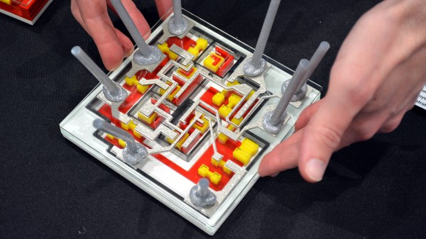
For years I’ve been trying to wrap my mind around how silicon chips actually work. How does a purposefully contaminated shard of glass wield control over electrons? Every once in a while, someone comes up with a learning aid that makes these abstract concepts really easy to understand, and this was the case with one of the booths at Maker Faire Bay Area. In addition to the insight it gave me (and hundreds of Faire-goers), here is an example of the best of what Maker Faire stands for. You’ll find a video of their presentation embedded below, along with closeup images of the props used at the booth.
The Uncovering the Silicon booth had a banner and a tablecloth, but was otherwise so unassuming that many people I spoke with missed it. Windell Oskay, Lenore Edman, Eric Schlepfer, John McMaster, and Ken Shirriff took a 50-year-old logic chip and laid it bare for anyone who cared to stop and ask what was on display. The Fairchild μL914 is a dual NOR gate, and it’s age matters because the silicon is not just simple, it’s enormous by today’s standards making it relatively easy to peer inside with tools available to the individual hacker.
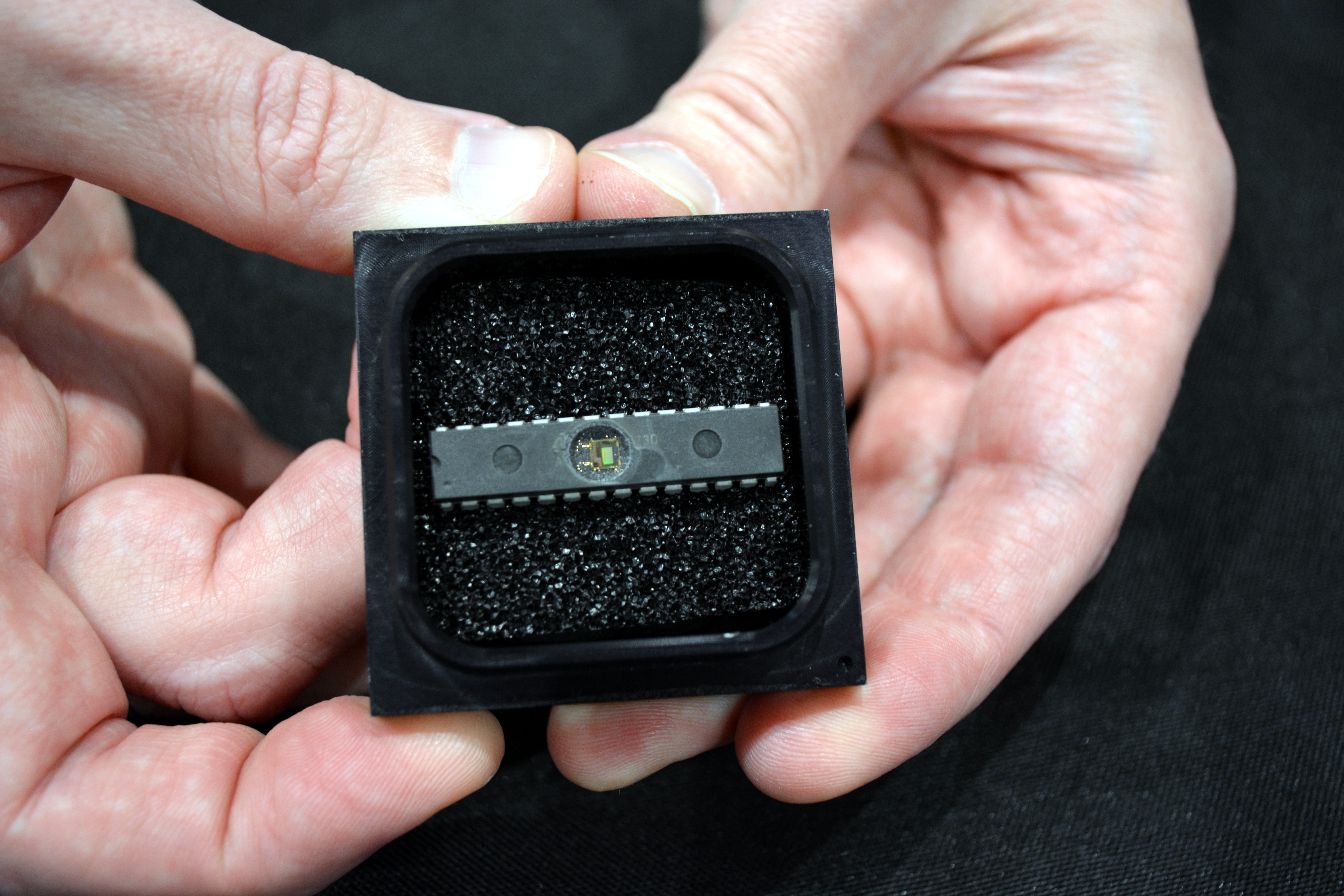
ATmega328 decapped by John McMaster was also on display at this booth
The first challenge is just getting to the die itself. This is John McMaster’s specialty, and you’re likely familiar from his Silicon Pr0n website. He decapped the chip (as well as an ATmega328 which was running the Arduino blink sketch with it’s silicon exposed). Visitors to the booth could look through the microscope and see the circuit for themselves. But looking doesn’t mean understanding, and that’s where this exhibit shines.
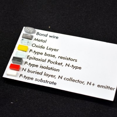
To walk us through how this chip works, a stack-up of laser-cut acrylic demonstrates the base, emitter, and collector of a single transistor. The color coding and shape of this small model makes it easy to pick out the six transistors of the 941 on a full model of the chip. This lets you begin to trace out the function of the circuit.
For me, a real ah-ha moment was the resistors in the design. A resistive layer is produced by doping the semiconductor with impurities, making it conduct more poorly. But how do you zero-in on the desired resistance for each part? It’s not by changing the doping, that remains the same. The trick is to make the resistor itself take up a larger footprint. More physical space for the electrons to travel means a lower resistance, and in the model you can see a nice fat resistor in the lower right. The proof for these models was the final showpiece of the exhibit as the artwork of the silicon die was laid out as a circuit board with discrete transistors used to recreate the functionality of the original chip.
Windell takes us through the booth presentation in the video below. I think you’ll be impressed by the breakdown of these concepts and how well they aid in understanding. This was a brilliant concept for an exhibit; it brought together interdisciplinary experts whom I respect and whose work I follow, and sought to invite everyone to gain a better understanding of the secrets hiding in the chips that underpin this technological age. This is exactly the kind of thing I love to see at a Maker Faire.
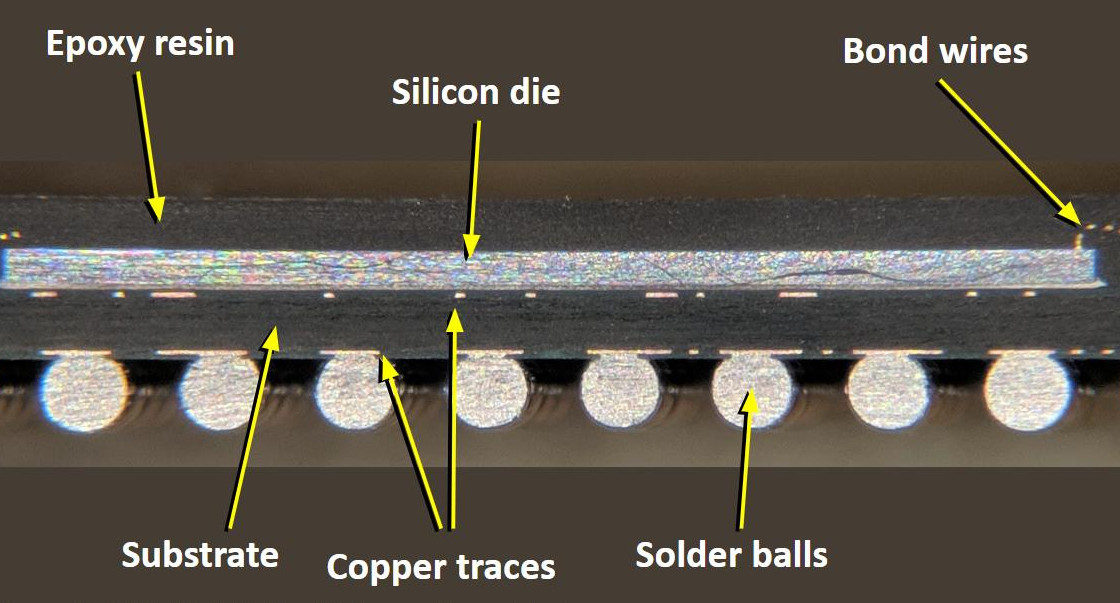
You may have heard the phrase “flip-chip” before: it’s a broad term referring to several integrated circuit packaging methods, the common thread being that the semiconductor die is flipped upside down so the active surface is closest to the PCB. As opposed to the more traditional method in which the IC is face-up and connected to the packaging with bond wires, this allows for ultimate packaging efficiency and impressive performance gains. We hear a lot about advances in the integrated circuits themselves, but the packages that carry them and the issues they solve — and sometimes create — get less exposure.
Cutaway view of traditional wire-bond BGA package. Image CC-BY-SA 4.0 @TubeTimeUS
Let’s have a look at why semiconductor manufacturers decided to turn things on their head, and see how radioactive solder and ancient Roman shipwrecks fit in.
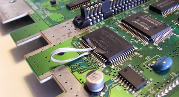
What do you do when you’re working with some vintage ICs and one of the tiny legs pops off? That’s what happened to [Kotomi] when working with an old Super Nintendo. A single lead for the sound chip just snapped off, leaving [Kotomi] one pin short of a working system (the Google Translatrix). This is something that can be fixed, provided you have a steady hand and a rotary tool that’s spinning at thousands of RPM.
Fixing this problem relies on a little bit of knowledge of how integrated circuits are built. There’s a small square of silicon in there, but this tiny die is bonded to a metal leadframe, which looks like the ribcage of a robotic centipede. This leadframe is covered in epoxy, the pins are bent down, and you have an IC. Removing just a tiny bit of epoxy grants access to the leadframe which you can then solder to. Don’t breathe the repair, it’s not pretty, but it does work.
While this technique makes use of a Dremel to break into the chewy nougat center of a vintage chip, and in some ways this could be called decapsulation, it really isn’t. We’ve seen people drop acid to get to the center of a chip and a really hot torch will get to the middle of a ceramic chip, but this technique is just accessing the lead frame of the IC. All ICs have a stamped (or photoetched) metal frame to which the silicone die is bonded. Running a Dremel against some epoxy doesn’t access the silicon, but it does grant access to the signals coming off the chip.
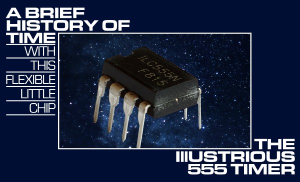
There’s a certain minimum set of stuff the typical Hackaday reader is likely to have within arm’s reach any time he or she is in the shop. Soldering station? Probably. Oscilloscope? Maybe. Multimeter? Quite likely. But there’s one thing so basic, something without which countless numbers of projects would be much more difficult to complete, that a shop without one or a dozen copies is almost unthinkable. It’s the humble 555 timer chip, a tiny chunk of black plastic with eight leads that in concert with just a few extra components can do everything from flashing an LED a couple of times a second to creating music and sound effects.
We’ve taken a look under the hood of the 555 before and featured many, many projects that show off the venerable chip’s multiple personalities quite well. But we haven’t looked at how Everyone’s First Chip came into being, and what inspired its design. Here’s the story of the 555 and how it got that way.