Few Things Are Cheaper Than This Antenna

As far as hobbies go, ham radio tends to be on the more expensive side. A dual-band mobile radio can easily run $600, and a high-end HF base station with the capability of more than 100 watts will easily be in the thousands of dollars. But, like most things, there’s an aspect to the hobby that can be incredibly inexpensive and accessible to newcomers. Crystal radios, for example, can be built largely from stuff most of us would have in our parts drawers, CW QRP radios don’t need much more than that, and sometimes even the highest-performing antennas are little more than two lengths of wire.

For this specific antenna, [W3CT] is putting together an inverted-V which is a type of dipole antenna. Rather than each of the dipole’s legs being straight, the center is suspended at some point relatively high above ground with the two ends closer to the earth. Dipoles, including inverted-Vs, are resonant antennas, meaning that they don’t need any tuning between them and the radio so the only thing needed to match the antenna to the feed line is a coax-to-banana adapter. From there it’s as simple as attaching the two measured lengths of wire for the target band and hoisting the center of the antenna up somehow. In [W3CT]’s case he’s using a mast which would break the $8 budget, but a tree or building will do just as well.

The video on the construction of this antenna goes into great detail, so if you haven’t built a dipole yet or you’re just getting started on your ham radio journey, it’s a great place to get started. From there we’d recommend checking out an off-center-fed dipole which lets a dipole operate efficiently on multiple bands instead of just one, and for more general ham radio advice without breaking the bank we’d always recommend the $50 Ham series.

Continue reading “Few Things Are Cheaper Than This Antenna”

A Simple Guide To RF PCB Design

[Hans Rosenberg] knows a thing or two about RF PCB design and has provided a three-part four-part video demonstration of some solid rules of thumb. We will cover the first part here and leave the other two for the more interested readers!

The design process begins with a schematic diagram, assuming ideal conductors. Advanced software tools can extract the resistive, inductive, and capacitive elements of the physical wiring to create a parasitic model that can be compared to the desired schematic. The RF designer’s task is to optimize the layout to minimize differences and achieve the best performance to meet the design goals. However, what do you do when you don’t have access to such software?

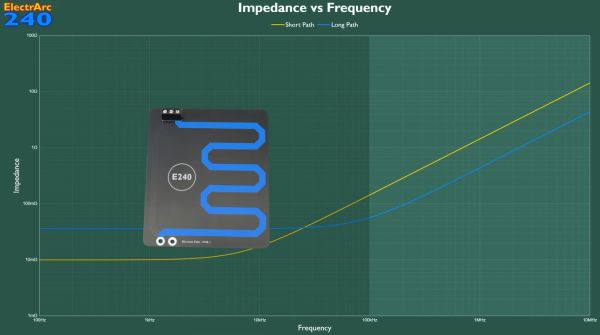
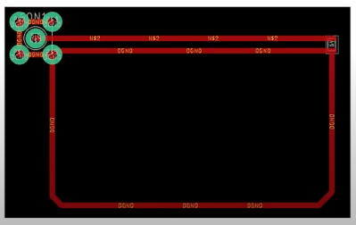
[Hans] explains that at low frequencies, return current flows through all paths, with the lowest resistance path taking most of the current. At higher frequencies, the lowest inductance path carries all the current. In real designs, a ground plane is used instead of an explicit return trace for the lowest possible impedance.

You really wouldn’t design an RF circuit like this.

[Hans] shows the effect of interrupting the signal return path on a physical test PCB. The result is pretty bad, with the current forced to detour around the hole in the ground plane. A nanoVNA shows a -20 dB drop at 4 GHz, where the ground plane has effectively become an antenna. Energy will be radiated out, causing signal loss, but worse, it will create an EMC hazard with an unintended transmission.

Additionally, this creates an EMC susceptibility, making the situation worse. Placing a solder blob to bridge the gap directly under the signal trace is all that’s required to make it a continuous straight path again, and the performance is restored.

Floating planes are also an issue in RF designs, causing signal resonance and losses. One solution is to pull back the planes near the signal or stitch them to the ground plane with vias placed closely on either side of the signal trace. However, such stitching may slightly affect transmission line impedance and require tweaking the design a little. The next two parts of the series expand on this, hammering home the importance of good ground plane design. These are definitely worth a watch!

PCB design is as much art as science, and we’ve discussed this subject a lot. Here’s our simple guide to rocking RF PCB designs. There’s also a lot of devil in that detail, for example when understanding edge-launch SMA connectors.

Continue reading “A Simple Guide To RF PCB Design”

Coax Stub Filters Demystified

Unless you hold a First Degree RF Wizard rating, chances are good that coax stubs seem a bit baffling to you. They look for all the world like short circuits or open circuits, and yet work their magic and act to match feedline impedances or even as bandpass filters. Pretty interesting behavior from a little piece of coaxial cable.

If you’ve ever wondered how stub filters do their thing, [Fesz] has you covered. His latest video concentrates on practical filters made from quarter-wavelength and half-wavelength stubs. Starting with LTspice simulations, he walks through the different behaviors of open-circuit and short-circuit stubs, as well as what happens when multiple stubs are added to the same feedline. He also covers a nifty online calculator that makes it easy to come up with stub lengths based on things like the velocity factor and characteristic impedance of the coax.

It’s never just about simulations with [Fesz], though, so he presents a real-world stub filter for FM broadcast signals on the 2-meter amateur radio band. The final design required multiple stubs to get 30 dB of attenuation from 88 MHz to 108 MHz, and the filter seemed fairly sensitive to the physical position of the stubs relative to each other. Also, the filter needed a little LC matching circuit to move the passband frequency to the center of the 2-meter band. All the details are in the video below.

It’s pretty cool to see what can be accomplished with just a couple of offcuts of coax. Plus, getting some of the theory behind those funny little features on PCBs that handle microwave frequencies is a nice bonus. This microwave frequency doubler is a nice example of what stubs can do.

Continue reading “Coax Stub Filters Demystified”

Homebrew TEM Cell Lets You EMC Test Your Own Devices

Submitting a new device for electromagnetic compatibility (EMC) testing seems a little like showing up for the final exam after skipping all the lectures. You might get lucky and pass, but it really would have been smarter to take a few of the quizzes to see how things were going during the semester. Similarly, it would be nice to know you’re not making any boneheaded mistakes early in the design process, which is what this DIY TEM cell is all about.

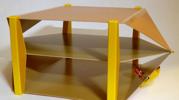
We really like [Petteri Aimonen]’s explanation of what a TEM cell, or transverse electromagnetic cell, is: he describes it as “an expanded coaxial cable that is wide enough to put your device inside of.” It basically a cage made of conductive material that encloses a space for the device under test, along with a stripline going down its center. The outer cage is attached to the outer braid of a coaxial cable, while the stripline is connected to the center conductor. Any electric or magnetic field generated by the device inside the cage goes down the coax into your test instrument, typically a spectrum analyzer.

[Petteri]’s homebrew TEM is made from a common enough material: copper-clad FR4. You could use double-sided material, or even sheet copper if you’re rich, but PCB stock is easy to work with and gets the job done. His design is detailed in a second post, which goes through the process of designing the size and shapes of all the parts as well as CNC milling the sheets of material. [Petteri] tried to make the joints by milling part-way through the substrate and bending the sheet into shape, but sadly, the copper didn’t want to cooperate with his PCB origami. Luckily, copper foil tape and a little solder heal all wounds. He also incorporated a line impedance stabilization network (LISN) into the build to provide a consistent 50-ohm characteristic impedance.

How does it work? Pretty well, it seems; when connected to a TinySA spectrum analyzer, [Petteri] was able to find high-frequency conductive noise coming from the flyback section of a switch-mode power supply. All it took was a ferrite bead and cap to fix it early in the prototyping phase of the project. Sounds like a win to us.

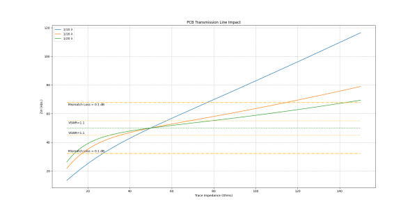
Input impedance plottet as a function of trace impedance for trace lengths of 1/10, 1/16 and 1/20 of a wavelength. (Credit: Baltic Labs)

When Does Impedance Matching A PCB Trace Become Unavoidable?

A common joke in electronics is that every piece of wire and PCB trace is an antenna, with the only difference being whether this was intentional or not. In practical terms, low-frequency wiring is generally considered to be ‘safe’, while higher frequency circuits require special considerations, including impedance (Z) matching.  Where the cut-off is between these two types of circuits is not entirely clear, however, with various rules-of-thumb in existence, as [Sebastian] over at Baltic Lab explains.

A popular rule is that no impedance matching between the trace and load is necessary if the critical length of a PCB trace (lcrit) is 1/10th of the wavelength (λ). Yet is this rule of thumb correct? Running through a number of calculations it’s obvious that the only case where the length of the PCB trace doesn’t matter is when trace and load impedance are matched.

According to these calculations, the 1/10 rule is not a great pick if your target is a mismatch loss of less than 0.1 dB, with 1/16 being a better rule. Making traces wider on the PCB can be advisable here, but ultimately you have to know what is best for your design, as each project has its own requirements. Even when the calculations look good, that’s no excuse to skip the measurement on the physical board, especially with how variable the dielectric constant of FR4 PCB material can be between different manufacturers and batches.

Heading image: Input impedance plotted as a function of trace impedance for trace lengths of 1/10, 1/16, and 1/20 of a wavelength. (Credit: Baltic Labs)

Continue reading “When Does Impedance Matching A PCB Trace Become Unavoidable?”

The Dipole Antenna Isn’t As Simple As It Appears

Dipole antennas are easy, right? Just follow the formula, cut two pieces of wire, attach your feedline, and you’re on the air.  But then again, maybe not. You’re always advised to cut the legs a little long so you can trim to the right length, but why? Shouldn’t the math just be right? And what difference does wire choice make on the antenna’s characteristics? The simple dipole isn’t really that simple at all.

If you’ve got antenna questions, check out [FesZ]’s new video on resonant dipoles, which is a deep dive into some of the mysteries of the humble dipole. In true [FesZ] fashion, he starts with simulations of various dipole configurations ranging from the ideal case — a lossless conductor in free space with as close to zero diameter conductors as the MMANA antenna simulator can support — and gradually build up to more practical designs. Continue reading “The Dipole Antenna Isn’t As Simple As It Appears”

Measuring Impedance Virtually

We always enjoy a [FesZ] video and we wonder if the “Z” stands for impedance? That’s the topic of his latest video series: measuring impedance with LTSpice. Of course, he also does his usual thorough job of mapping the virtual world to the real one. You can see the video below.

It is simple enough. Impedance is very similar to resistance. That is to say, we have a ratio of voltage and current. However, since it is an AC quantity, you need a complex number to represent it and there is an associated phase shift.

Continue reading “Measuring Impedance Virtually”