Your Own Core Rope Memory

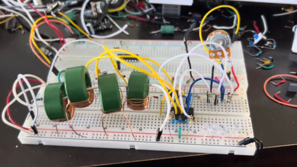
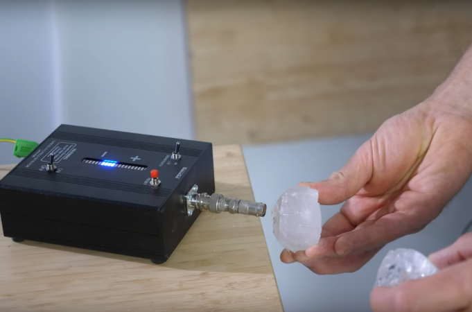
If you want read-only memory today, you might be tempted to use flash memory or, if you want old-school, maybe an EPROM. But there was a time when that wasn’t feasible. [Igor Brichkov] shows us how to make a core rope memory using a set of ferrite cores and wire. This was famously used in early UNIVAC computers and the Apollo guidance computer. You can see how it works in the video below.

While rope memory superficially resembles core memory, the principle of operation is different. In core memory, the core’s magnetization is what determines any given bit. For rope memory, the cores are more like a sensing element. A set wire tries to flip the polarity of all cores. An inhibit signal stops that from happening except on the cores you want to read. Finally, a sense wire weaves through the cores and detects a blip when a core changes polarity. The second video, below, is an old MIT video that explains how it works (about 20 minutes in).

Why not just use core memory? Density. These memories could store much more data than a core memory system in the same volume. Of course, you could write to core memory, too, but that’s not always a requirement.

We’ve seen a resurgence of core rope projects lately. Regular old core is fun, too.

Continue reading “Your Own Core Rope Memory”

A Delay Line Memory Demo Board

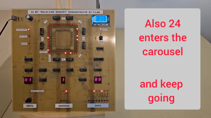
Delay line memory is a technology from yesteryear, but it’s not been entirely forgotten. [P-Lab] has developed a demo board for delay-line memory, which shows how it worked in a very obvious way with lots of visual aids.

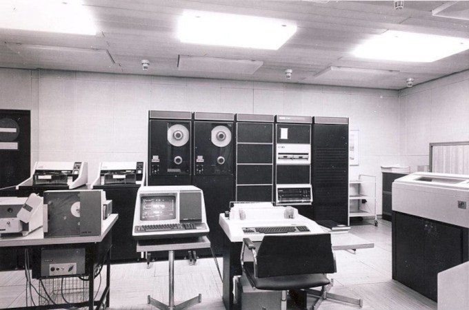
If you’re unfamiliar with the technology, it’s a form of memory that was used in classic computers like the Univac-I and the Olivetti Programma 101. It’s a sequential-access technology, where data is stored as pulses in some kind of medium, and read out in order. Different forms of the technology exist, such as using acoustic pulses in mercury or torsional waves passing through coiled nickel wire.

In this case, [P-Lab] built a solid state delay line using TTL ICs, capable of storing a full 64 bits of information and running at speeds of up to 150 kHz. It also features a write-queuing system to ensure bits are written at the exact correct time — the sequential-access nature of the technology means random writes and reads aren’t actually possible. The really cool thing is that [P-Lab] paired the memory with lots of LEDs to show how it works. There are lights to indicate the operation of the clock, and the read and write cycles, as well as individual LEDs indicating the status of each individual bit as they roll around the delay line. Combined with the hexadecimal readouts, it makes it easy to get to grips with this old-school way of doing things.

We’ve seen previous work from[P-Lab] in this regard using old-school core rope memory, too. Continue reading “A Delay Line Memory Demo Board”

Fitting A Spell Checker Into 64 KB

By some estimates, the English language contains over a million unique words. This is perhaps overly generous, but even conservative estimates generally put the number at over a hundred thousand. Regardless of where the exact number falls between those two extremes, it’s certainly many more words than could fit in the 64 kB of memory allocated to the spell checking program on some of the first Unix machines. This article by [Abhinav Upadhyay] takes a deep dive on how the early Unix engineers accomplished the feat despite the extreme limitations of the computers they were working with.

Perhaps the most obvious way to build a spell checker is by simply looking up each word in a dictionary. With modern hardware this wouldn’t be too hard, but disks in the ’70s were extremely slow and expensive. To move the dictionary into memory it was first whittled down to around 25,000 words by various methods, including using an algorithm to remove all affixes, and then using a Bloom filter to perform the lookups. The team found that this wasn’t a big enough dictionary size, and had to change strategies to expand the number of words the spell checker could check. Hash compression was used at first, followed by hash differences and then a special compression method which achieved an almost theoretically perfect compression.

Although most computers that run spell checkers today have much more memory as well as disks which are orders of magnitude larger and faster, a lot of the innovation made by this early Unix team is still relevant for showing how various compression algorithms can be used on data in general. Large language models, for one example, are proving to be the new frontier for text-based data compression.

Dog Plays Chess On ESP32

The ESP32 is s remarkably powerful microcontroller, where its dual-core processor and relatively high clock speed can do some impressive work. But getting this microcontroller designed for embedded systems to do tasks that would generally be given to a much more powerful PC-type computer takes a little bit more willpower. Inspired by his dog, [Folkert] decided to program an ESP32 to play chess, a famously challenging task for computer scientists in the past. He calls this ESP32 chess system Dog.

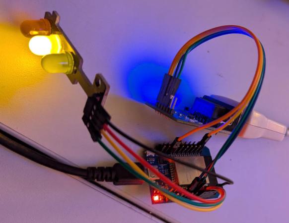
One of the other major limitations of this platform for a task like this is memory. The ESP32 [Folkert] is using only has 320 kB of RAM, so things like the transposition table have to fit in even less space than that. With modern desktop computers often having 32 or 64 GB, this is a fairly significant challenge, especially for a memory-intensive task like a chess engine. But with the engine running on the microcontroller it’s ready to play, either in text mode or with something that can use the Universal Chess Interface (UCI). A set of LEDs on the board lets the user know what’s going on while gameplay is taking place.

Continue reading “Dog Plays Chess On ESP32”

Quake In 276 KB Of RAM

Porting the original DOOM to various pieces of esoteric hardware is a rite of passage in some software circles. But in the modern world, we can get better performance than the 386 processor required to run the 1993 shooter for the cost of a dinner at a nice restaurant — with plenty of other embedded systems blowing these original minimum system requirements out of the water.

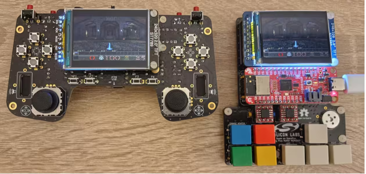
For a much tougher challenge, a group from Silicon Labs decided to port DOOM‘s successor, Quake, to the Arduino Nano Matter Board platform instead even though this platform has some pretty significant limitations for a game as advanced as Quake.

To begin work on the memory problem, the group began with a port of Quake originally designed for Windows, allowing them to use a modern Windows machine to whittle down the memory usage before moving over to hardware. They do have a flash memory module available as well, but there’s a speed penalty with this type of memory. To improve speed they did what any true gamer would do with their system: overclock the processor. This got them to around 10 frames per second, which is playable, but not particularly enjoyable. The further optimizations to improve the FPS required a much deeper dive which included generating lookup tables instead of relying on computation, optimizing some of the original C programming, coding some functions in assembly, and only refreshing certain sections of the screen when needed.

On a technical level, Quake was a dramatic improvement over DOOM, allowing for things like real-time 3D rendering, polygonal models instead of sprites, and much more intricate level design. As a result, ports of this game tend to rely on much more powerful processors than DOOM ports and this team shows real mastery of their hardware to pull off a build with a system with these limitations. Other Quake ports we’ve seen like this one running on an iPod Classic require a similar level of knowledge of the code and the ability to use assembly language to make optimizations.

Thanks to [Nicola] for the tip!

Giving The Original Xbox 256 MB Of Memory

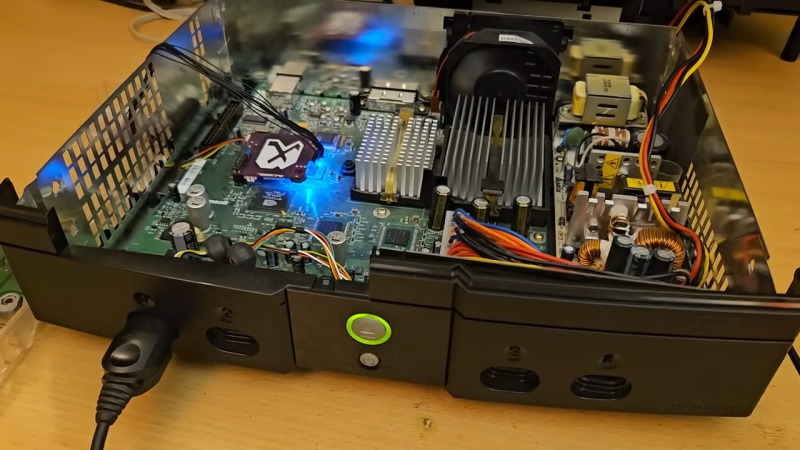
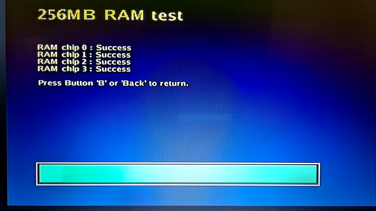
The original Xbox forever changed the console world, because it was basically just PC components laced together in a slightly different architecture. It featured a Pentium 733 MHz CPU with just 64MB of RAM. [Prehistoricman] has been hard at work, figuring out how to up that to 256MB instead.

This isn’t [Prehistoricman’s] first rodeo. Previously, he managed to up the Xbox’s RAM to 128 MB. To figure out how to go further, he had to figure out the addressing scheme. A datasheet for the Xbox’s original memory chip was a help in this regard, as was the envytools project and an Xbox source code leak.

A BIOS hack was needed to move the auto-precharge pin to free up more address pins for the higher memory space. Furthermore, the only available memory chips that were suitable used BGA packages, so a small PCB with castellated edges was needed to adapt the chip to the Xbox’s motherboard, which expects a TQFP package.

Ultimately, getting this hack to work involved a lot of bare-metal hacking. It also won’t help the performance of commercial games at all, as they were all designed within the limitations of the original console. Still, it’s impressive to see this now-ancient platform hacked to do more. It’s also hilarious to compare it with a contemporary PC, which could simply accept 256 MB of RAM by using additional memory slots. Video after the break.

Continue reading “Giving The Original Xbox 256 MB Of Memory”

Build Your Own Core Rope Memory Module?

[Luizão] wanted to create some hardware to honour the memory of the technology used to put man on the moon and chose the literal core of the project, that of the hardware used to store the software that provided the guidance. We’re talking about the magnetic core rope memory used in the Colossus and Luminary guidance computers. [Luizão] didn’t go totally all out and make a direct copy but instead produced a scaled-down but supersized demo board with just eight cores, each with twelve addressable lines, producing a memory with 96 bits.

The components chosen are all big honking through-hole parts, reminiscent of those available at the time, nicely laid out in an educational context. You could easily show someone how to re-code the memory with only a screwdriver to hand; no microscope is required for this memory. The board was designed in EasyEDA, and is about as simple as possible. Being an AC system, this operates in a continuous wave fashion rather than a pulsed operation mode, as a practical memory would. A clock input drives a large buffer transistor, which pushes current through one of the address wires via a 12-way rotary switch. The cores then act as transformers. If the address wire passes through the core, the signal is passed to the secondary coil, which feeds a simple rectifying amplifier and lights the corresponding LED. Eight such circuits operate in parallel, one per bit. Extending this would be easy.

Continue reading “Build Your Own Core Rope Memory Module?”