Pretty purple PCBs, made in the USA

Does Made-in-America Make Sense For PCB Prototyping?

These are tough times for American hackers, and rife with uncertainty. Trade wars are on, off, on again– who can keep track? If you’re used to getting everything from China, that can really cramp your style. [Jeremy Cook] took the time to write up his experience prototyping with American-made PCBs , just in time for us to totally miss Independence Day.

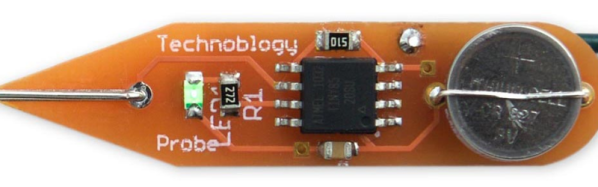
The project was a simple nightlight, using a single LED, a photoresistor, a transistor, and a CR2032 battery. The CR2032 battery does complicate things, though: [Jeremy] figured out a neat way to hold the battery using a PCB cutout, but it needs to be a 0.8 mm board. (That’s going to matter in a moment.) He’s put that PCB on GitHub if you’re interested.

To start off, JLBPCB is the Chinese clearing house of choice for [Jeremy], and they quoted a very cheap $7.10 for 20 boards. The problem was that shipping across the Pacific Ocean, plus the ever-wavering tariff charge, brought the price to $48.08. About five dollars of which was from tariffs; the rest you can put down to the cost of jet fuel and the size of the Pacific Ocean.

On the other hand, OSH Park, was able to get [Jeremy] three of their pretty purple PCBs for $7.75 all-inclusive. Overall, since he’s prototyping and does not want 20 boards this revision, [Jeremy] saves quite a lot by staying local– including the environmental impact of shipping and laxer regulations in China, if that sort of thing matters to you. 

The suprizing thing is the turnaround time: [Jeremy] got his pretty purple PCBs from OSH Park a full twenty days after ordering. Similar orders from China take only a week, which is just mind-blowing when you stop and think about the great honking ocean in the way. We could perhaps cut OSH Park some slack in that 0.8 mm boards are not the most common, but their quoted turnaround time for two-layer prototypes is minimum 12 days.

They do offer a “super-swift” option for two-layer boards, but then they lose on price. As [Jeremy] points out, there are always tradeoffs. If you’re really in a hurry, nothing’s faster than milling the boards yourself. Or you could go the old-school toner-transfer etching route.

Our thanks to [Jeremy] for the tip. If you’ve got a better way to prototype, do send us a tip about it. Also, please us know in the comments if you’ve tried an in-country PCB fabricator, and how it compared to the usual offerings from the PRC.

Discrete LEDs Make A Micro Display

Few things excite a Hackaday staff member more than a glowing LED, so it should be no surprise that combining them together into a matrix really gets us going. Make that matrix tiny, addressable, and chainable and you know it’ll be a hit at the virtual water cooler. We’ve seen [tinyledmatrix]’s work before but he’s back with the COPXIE, a pair of tiny addressable displays on one PCBA.

The sample boards seen at top are a particularly eye catching combination of OSH Park After Dark PCB and mysterious purple SMT LEDs that really explain the entire premise. Each PCBA holds two groups of discrete LEDs each arranged into a 5×7 display. There’s enough density here for a full Latin character set and simple icons and graphics, so there should be enough flexibility for all the NTP-synced desk clocks and train timetables a temporally obsessed hacker could want.

Continue reading “Discrete LEDs Make A Micro Display”

New Contest: Flexible PCBs

The now-humble PCB was revolutionary when it came along, and the whole ecosystem that evolved around it has been a game changer in electronic design. But the PCB is just so… flat. Planar. Two-dimensional. As useful as it is, it gets a little dull sometimes.

Here’s your chance to break out of Flatland and explore the third dimension of circuit design with our brand new Flexible PCB Contest.

We’ve teamed up with Digi-Key for this contest. Digi-Key’s generous sponsorship means 60 contest winners will receive free fabrication of three copies of their flexible PCB design, manufactured through the expertise of OSH Park. So now you can get your flex on with wearables, sensors, or whatever else you can think of that needs a flexible PCB.

Continue reading “New Contest: Flexible PCBs”

PCB Take On Stars, Moons, And Ringed Planets Is Gold

Remember when PCBs were green and square? That’s the easy default, but most will agree that when you’re going to show off your boards instead of hiding them in a case, it’s worth extra effort to make them beautiful. We’re in a renaissance of circuit board design and the amount of effort being poured into great looking boards is incredible. The good news is that this project proves you don’t have to go nuts to achieve great results. This stars, moons, and planets badge looks superb using just two technical tricks: exposed (plated) copper and non-rectangular board outline.

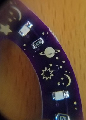
Don’t take that the wrong way, there’s still a lot of creativity that [Steve] over at Big Mess o’ Wires used to make it look this great. The key element here is that copper and solder mask placements have extremely fine pitch. After placing the LEDs and resistors there’s a lot of blank space which was filled with what you might see in the night sky through your telescope.  What caught our eye about this badge is the fidelity of the ringed planet.

The white ink of silk screen is often spotty and jagged at the edges. But this copper with ENIG (gold) plating is crisp through the curves and with razor-sharp tolerance. It’s shown here taken under 10x magnification and still holds up. This is a trick to keep under your belt — if you have ground pours it’s easy to spice up the look of your boards just by adding negative-space art in the solder mask!

[Steve] mentions the board outline is technically not a circle but “a many-sided polygon” due to quirks of Eagle. You could have fooled us! We do like how he carried the circle’s edges through the bulk of the board using silk screen. If you’re looking for tips on board outline and using multiple layers of art in Eagle, [Brian Benchoff] published a fabulous How to do PCB art in Eagle article. Of course, he’s gone deeper than what the board houses offer by grabbing his own pad printing equipment and adding color to white solder mask.

The art was the jumping off point for featuring this badge, but [Steve] is known for his technical dives and this one is no different. He’s done a great job of recounting everything that popped up while designing the circuit, from LED color choice to coin cell internal resistance and PWM to low-power AVR tricks.

Friday Hack Chat: Everything PCB

It was not too long ago that all PCB design packages were proprietary. Getting PCBs made was expensive, and if you tried to do this over the Internet, the best way was to download a board house’s proprietary software, design your board in their software suite, and send your boards off to be made. A 5 cm square board would cost two hundred dollars. I know this to be true because I’ve said it before, and no one has corrected me.

For this week’s Hack Chat, we’re talking Everything PCB with OSH Park. OSH Park is the leading creators of perfect purple PCBs. They have POGs, and for the last two weeks, they’ve been one of the few places you can send some Gerbers to and have it manufactured in a timely manner if you live in the US. Because China was closed.

For this week’s Hack Chat, we’re going to be talking about everything PCB. How do you do castellated holes? How do you mill slots and square or otherwise non-round holes? Internal cutouts? Stop mask expansion? Artwork? Panelization? Why purple? More POGs!

Our guests for this chat will be [Dan Sheadel] and [Drew Fustini] of OSH Park, and they’re going to be there answering all your questions. [Dan] has been around OSH Park from the beginning and enjoys designing tiny useless robots and mentoring students building better ones. [Drew] is an Open Source hardware developer, firmware designer, a BeagleBoard board member, and is usually found at hardware meetups wearing purple.

join-hack-chat

Our Hack Chats are live community events on the Hackaday.io Hack Chat group messaging. This Hack Chat is going down Friday, March 2nd at noon, Pacific time. Want to know what time this is happening in your neck of the woods? Have a countdown timer!

Click that speech bubble to the right, and you’ll be taken directly to the Hack Chat group on Hackaday.io.

You don’t have to wait until Friday; join whenever you want and you can see what the community is talking about.

These Small PCBs Are Made For Model Rocketry

Model rocketry hobbyists are familiar with the need to roll their own solutions when putting high-tech features into rockets, and a desire to include a microcontroller in a rocket while still keeping things flexible and modular is what led [concretedog] to design a system using 22 mm diameter stackable PCBs designed to easily fit inside rocket bodies. The system uses a couple of 2 mm threaded rods for robust mounting and provides an ATTiny85 microcontroller, power control, and an optional small prototyping area. Making self-contained modular sleds that fit easily into rocket bodies (or any tube with a roughly one-inch inner diameter) is much easier as a result.

The original goal was to ease the prototyping of microcontroller-driven functions like delayed ignition or altimeter triggers in small Estes rockets, but [concretedog] felt there were probably other uses for the boards as well and made the design files available on GitHub. (Thanks!)

We have seen stackable PCBs for rocketry before with the amazingly polished M3 Avionics project, but [concretedog]’s design is much more accessible to some hobbyist-level tinkering; especially since the ATTiny85 can be programmed using the Arduino IDE and the boards themselves are just an order from OSH Park away.

[via Dangerous Prototypes Blog]


Continuity Tester Uses The ATtiny85’s Comparator

There’s an inside joke among cyclists – the number of bikes you need is “n+1”, where “n” is your current number of bikes. The same probably also applies to the number of tools and equipment a hacker needs on their workbench. Enough is never enough. Although [David Johnson-Davies] has a couple of multimeters lying around, he still felt the urge to build a stand-alone continuity tester and has posted details for a super-simple ATtiny85 based Continuity Tester on his blog. For a device this simple, he set himself some tall design goals. Using the ATtiny85 and a few SMD discretes, he built a handy tester that met all of his requirements and then some.

The ATtiny85’s Analog Comparator function is perfectly suited for such a tester. One input of the comparator is biased such that there is a 51 ohm resistor between the input and ground. The output of the comparator toggles when the resistance between the other input and ground is either higher or lower than 51 ohms. Enabling internal pullup resistors in the ATtiny85 not only takes care of proper biasing of the comparator pins, but also helps reduce current consumption when the ATtiny85 is put to sleep. The test current is limited to 100 μA, making the tester suitable for use in sensitive electronics. And enabling the sleep function after 60 seconds of inactivity reduces standby current to just about 1 μA, so there is no need for a power switch. [David] reckons the CR927 button cell ought to last pretty long.

For those interested in building this handy tester, [David] has shared the Eagle CAD files as well as the ATtiny85 code on his Github repository or you could just order out some boards from OSHpark.