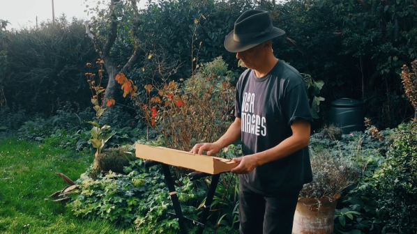
The Eowave Persephone was a beautiful thing—a monophonic ribbon synth capable of producing clean, smoothly varying tones. [Ben Glover] used to own a nice example that formerly belonged to Peter Christopherson, but lost it in the shifting sands of time. His solution was to build one of his own from scratch.
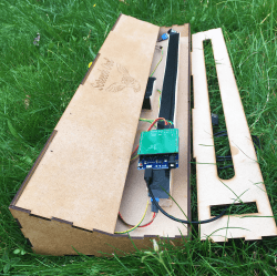
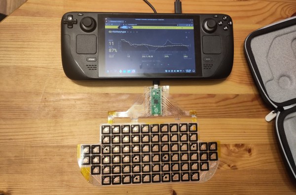
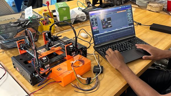
Known as the Screech Owl, the build is based around a custom shield designed to suit the Arduino Leonardo. The primary control interface is a Softpot 500 mm membrane potentiometer, layered up with a further thin film pressure sensor which provides aftertouch control. The Leonardo reads these sensors and synthesizes the appropriate frequencies in turn.
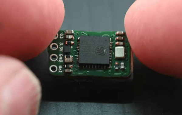
All the electronics is wrapped up inside a tidy laser-cut enclosure that roughly approximates the design of the original Eowave device. [Ben] noted the value of services like Fiverr and ChatGPT for helping him with the design, while he also enjoyed getting his first shield design professionally manufactured via JLCPCB.
It’s a tidy build, and in [Ben’s] capable hands, it sounds pretty good, too. We’ve seen some other great ribbon controlled synths before, too. Video after the break.
Continue reading “Screech Owl Is A Tribute To The Eowave Persephone”