PCB internal bodge

PCB Microsurgery Puts The Bodges Inside The Board

We all make mistakes, and there’s no shame in having to bodge a printed circuit board to fix a mistake. Most of us are content with cutting a trace or two with an Xacto or adding a bit of jumper wire to make the circuit work. Very few of us, however, will decide to literally do our bodges inside the PCB itself.

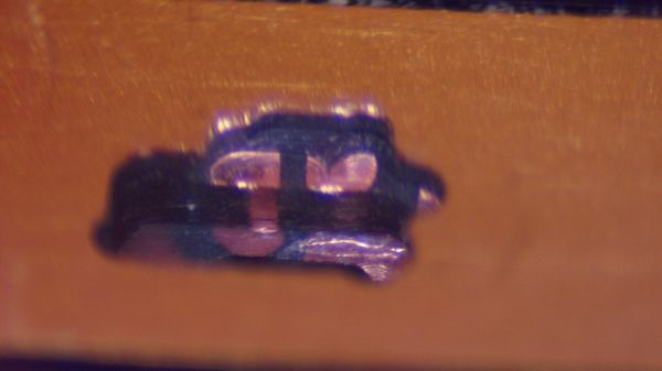
The story is that [Andrew Zonenberg] was asked to pitch in debugging some incredibly small PCBs for a prototype dev board that plugs directly into a USB jack. The six-layer boards are very dense, with a forest of blind vias. The Twitter thread details the debugging process, which ended up finding a blind via on layer two shorted to a power rail, and another via shorted to ground. It also has some beautiful shots of [Andrew]’s “mechanical tomography” method of visualizing layers by slowly grinding down the surface of the board.

[Andrew] has only tackled one of the bodges at the time of writing, but it has to be seen to be believed. It started with milling away the PCB to get access to the blind via using a ridiculously small end mill. The cavity [Andrew] milled ended up being only about 480 μm by 600 μm and only went partially through a 0.8-mm thick board, but it was enough to resolve the internal short and add an internal bodge to fix a trace that was damaged during milling. The cavity was then filled up with epoxy resin to stabilize the repair.

This kind of debugging and repair skill just boggles the mind. It reminds us a bit of these internal chip-soldering repairs, but taken to another level entirely. We can’t wait to see what the second repair looks like, and whether the prototype for this dev board can be salvaged.

Thanks to [esclear] for the heads up on this one.

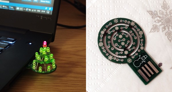
USB LED Christmas Tree Is Making Spirits Bright

[Piotr SB] knows there is no way out of the holidays; the only path is through. You’ve got to find cheer wherever and however you can, so why not cater to your own interests and build the cutest little LED Christmas tree you ever did see? And did we mention it’s USB and absolutely free (as in carols, not eggnog)?

This O-Christmas tree is made up of concentric rings that are built into a tier as you solder the LEDs. And of course you’re supposed use the LED legs as supports! One leg from each LED — 18 green and a red one for the top. Because the PCB is not quite thick enough, you’ll need to add a plastic spacer to get it to stay in the USB port. Not only is this a nice design, the snowflakes and snowman on the silkscreen totally seal the cuteness deal.

Ever get so frustrated with your Christmas tree that you want to just empty a few rounds into the thing? No? Well, you’d have a good reason to if you built this Duck Hunt ornament.

DIY castellated PCB connectors

Snip Your Way To DIY PCB Castellations

Castellated PCB edges are kind of magical. The plated semicircular features are a way to make a solid, low-profile connection from one board to another, and the way solder flows into them is deeply satisfying. But adding them to a PCB design isn’t always cheap. No worries there — you can make your own castellations with this quick and easy hack.

Scissors cutting a PCB through vias to make castellations[@CoilProtogen] doesn’t include much information in the Twitter thread about design details, but the pictures make it clear what the idea is here. OEM castellations are really just plated areas at the edge of a board that can be used to tack the board down to another one without any added hardware. The hack here is realizing that lining up a bunch of large-diameter vias and cleaving them in half with a sharp pair of scissors will result in the same profile without the added cost. The comments on the thread range from extolling the brilliance of this idea to cringing over the potential damage to the board, but [@CoilProtogen] insists that the 0.6-mm substrate cuts like butter. We’d worry that the plating on the vias would perhaps tear, but that seems not to be the case here.

The benefits of a zero-profile connection are pretty clear in this case, where castellated PCBs were used to replace bulky header-pin connectors on a larger PCB. We can see this technique being generally useful; we’ve seen them used to good effect before, and this is a technique we’ll keep in mind for later.

Lasers Make PCBs The Old Fashioned Way

There are many ways to create printed circuit boards, but one of the more traditional ways involves using boards coated with photoresist and exposing the desired artwork on the board, usually with UV light. Then you develop the board like a photograph and etch it in acid. Where the photoresist stays, you’ll wind up with copper traces. Hackers have used lots of methods to get that artwork ranging from pen plotters to laser printers, but commercially a machine called a photoplotter created the artwork using a light and a piece of film. [JGJMatt] sort of rediscovered this idea by realizing that a cheap laser engraver could directly draw on the photoresist.

The laser dot is about 0.2 mm in diameter, so fine resolution boards are possible. If you have a laser cutter or engraver already, you have just about everything you need. If not, the lower-power laser modules are very affordable and you can mount one on a 3D printer. Most people are interested in using these to cut where higher power is a must, but for exposing photosensitive film, you don’t need much power. The 500 mW module used in the project costs about fifty bucks.

Continue reading “Lasers Make PCBs The Old Fashioned Way”

Secret Ingredient For 3D-Printed Circuit Traces: Electroplating

Conductive filament exists, but it takes more than that to 3D print something like a circuit board. The main issue is that traces made from conductive filament are basically resistors; they don’t act like wires. [hobochild]’s interesting way around this problem is to use electroplating to coat 3D-printed traces with metal, therefore creating a kind of 3D-printed circuit board. [hobochild] doesn’t yet have a lot of nitty-gritty detail to share, but his process seems fairly clear. (Update: good news! here’s the project page and GitHub repository with more detail.)

The usual problem with electroplating is that the object to be coated needs to be conductive. [hobochild] addresses this by using two different materials to create his test board. The base layer is printed in regular (non-conductive) plastic, and the board’s extra-thick traces are printed in conductive filament. Electroplating takes care of coating the conductive traces, resulting in a pretty good-looking 3D-printed circuit board whose conductors feature actual metal. [hobochild] used conductive filament from Proto-pasta and the board is a proof-of-concept flashing LED circuit. Soldering might be a challenge given the fact that the underlying material is still plastic, but the dual-material print is an interesting angle that even allows for plated vias and through-holes.

We have seen conductive filament used to successfully print workable electrical connections, but applications are limited due to the nature of the filament. Electroplating, a technology accessible to virtually every hacker’s workbench, continues to be applied to 3D printing in interesting ways and might be a way around these limitations.

Slick Keyboard Built With PCB Magic

Sometimes a chance conversation leads you to discover something cool you’ve not seen before, and before you know it, you’re ordering parts for yet another hardware build. That’s what happened to this scribe the other day when chatting on some random discord, to QMK maintainer [Nick Brassel aka tzarc] about Djinn, a gorgeous 64-key split mechanical keyboard testbed. It’s a testbed because it uses the newest STM32G4x microcontroller family, and QMK currently does not have support for this in the mainline release. For the time being, [Nick] maintains a custom release, until it gets merged.

Hardware-wise, the design is fabulous, with a lot of attention to detail. We have individual per-key RGB LEDs, RGB underglow, a rotary encoder, a five-way tactile thumb switch, and a 240×320 LCD per half. The keyboard is based on a three PCB stack, two of which are there purely for structure. This slick design has enough features to keep a fair few of us happy.

Interestingly, when you look at the design files (KiCAD, naturally) [Nick] has chosen to take a mirrored approach to the PCB. That means the left and right sides are actually the same PCB layout. The components are populated on different sides of the PCB depending on which half you’re looking at! By mirroring footprints on both PCB sides, and hooking everything up in parallel, it’s possible to do it all with a single master layout.

This is a simple but genius idea that this scribe hadn’t come across before (the shame!) Secondarily it keeps costs down, as your typical Chinese prototyping house will not deal in PCB quantities below five, so you can make two complete keyboards on one order, rather than needing two orders to make five. (Yes, there are actually three unique PCBs, but we’re simplifying the situation, ok?)

Now, if only this pesky electronics shortage could abate a bit, and we could get the parts to build this beauty!

Obviously, we’ve covered many, many keyboards over the years. Here’s our own [Kristina’s] column all about the things. If you need a little help with your typing skills, this shocking example may be the one for you. If your taste is proper old-school clackers, there’s something for everyone.

PCB fluorescent 7-segment display

Unique Seven-Segment Display Relies On FR-4 Fluorescence

It’s interesting what you see when you train a black light on everyday objects. We strongly suggest not doing this in a hotel room, but if you shine UV light on, say, a printed circuit board, you might see what [Sam Ettinger] did, which led him to build these cool low-profile seven-segment fluorescent PCB displays.

UV light causing FR4 to fluoresceAs it turns out, at least some FR-4 PCBs fluoresce under UV light, giving off a ghostly blue-green glow. Seeing the possibilities, [Sam] designed a PCB with cutouts in the copper and solder mask in the shape of a traditional seven-segment display. The backside of the PCB has pads for UV LEDs and current-limiting resistors, which shine through the board and induce the segments to glow. Through-slots between the segments keep light from one segment from bleeding over into the next; while [Sam] left the slots unfilled, they could easily be filled with solder. The fluorescent property of FR-4, and therefore the brightness and tint of the segments, seems to vary by board thickness and PCB manufacturer, but it looks like most PCBs will show pretty good results.

We’d say the obvious first improvement might be to cover the back of the display with black epoxy, to keep stray light down, and to improve contrast. But they look pretty great just as they are. We can also see how displays with other shapes, like icons and simple symbols. Or maybe even alphanumeric characters — say, haven’t we seen something like that before?