Inductance In PCB Layout: The Good, The Bad, And The Fugly

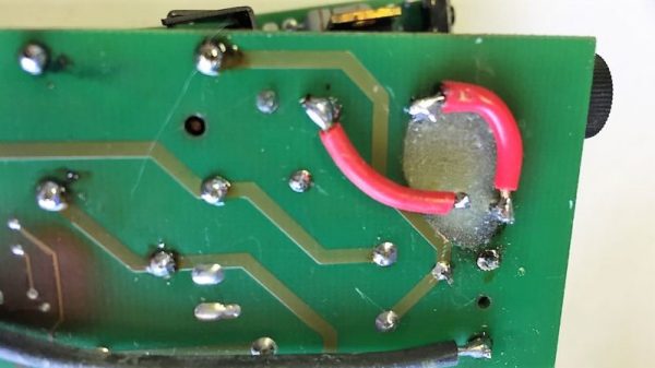
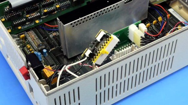
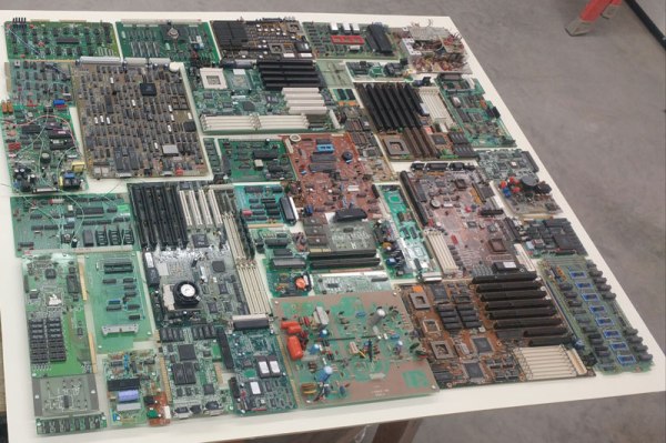
When current flows through a conductor it becomes an inductor, when there is an inductor there is an electromagnetic field (EM). This can cause a variety of issues during PCB layout if you don’t plan properly, and sometimes we get burned even when we think we have planned for unwanted inductance and the effects that come with them.

When doing high speed logic we need to be able to deliver sudden changes in current to the devices if we want to have proper switching times and logic levels. Unfortunately inductance is usually not a friend in these circumstances as it resists those sudden changes in current. If the high speed devices are driving capacitive loads, which themselves are resisting changes in voltage, even more instantaneous current is needed.

Simply put, inductors resist a change of current, and can act as a low pass filter when in series with the signal or power supply flow. Inductors do this by storing energy in the flux surrounding the conductor. Alternatively capacitors resist a change in voltage (again by storing energy) and can act as a high pass filter when in series with the signal. This makes them a valuable tool in the fight against unwanted inductance in power supply distribution.

In the video below, and the remainder of this article, I’m going to dive into the concept of inductance and how it affects our design choices when laying out circuit boards.

Continue reading “Inductance In PCB Layout: The Good, The Bad, And The Fugly”

Epoxy Fix For A Combusted PCB

When the Magic Smoke is released, chances are pretty good that you’ve got some component-level diagnosis to do. It’s usually not that hard to find the faulty part, charred and crusty as it likely appears. In that case, some snips, a new non-crusty part, and a little solder are usually enough to get you back in business.

But what if the smoke came not from a component but from the PCB itself? [Happymacer] chanced upon this sorry situation in a power supply for an electric gate opener. Basking in the Australian sunshine for a few years, the opener started acting fussy at first, then not acting at all. Inspection of its innards revealed that some unlucky ants had shorted across line and neutral on the power supply board, which burned not only the traces but the FR4 of the board as well. Rather than replace the entire board, [Happymacer] carefully removed the carbonized (and therefore conductive) fiberglass and resin, leaving a gaping hole in the board. He fastened a patch for the hole from some epoxy glue; Araldite is the brand he used, but any two-part epoxy, like JB Weld, should work. One side of the hole was covered with tape and the epoxy was smeared into the hole, and after a week of curing and a little cleanup, it was ready for duty. The components were placed into freshly drilled holes, missing traces were replaced with wire, and it seems to be working fine.

This seems like a great tip to keep in mind for when catastrophe strikes your boards. There are more extreme ways to do it, of course, but perhaps none so flexible. After all, epoxy is versatile stuff.

Touch Anything And Everything

Powering IoT devices is often a question of batteries or mains power, but in rare exceptions to this rule there is no power supply (PDF Warning). At the University of Wisconsin-Madison and the University of California, San Diego, researchers have gone the extra mile to make advanced backscatter devices, and these new tags don’t need the discrete components we have seen in previous versions. They are calling it LiveTag, and it doesn’t need anything aside from a layer of foil printed or etched on a flexible ceramic-PTFE laminate. PTFE is mostly seen in the RF sector as a substrate for circuit boards.

We have seen some of the wild creations with wifi backscatter that range from dials to pushbuttons. RF backscatter works by modulating the RF signals in which we are continuously swimming. Those radio waves power the device and disrupt the ambient signals, which disruption can be detected by a receiver. With a BOM that looks like a statement more than a list, integration with many devices becomes a cost-effective reality. Do not however broadcast important data because you cannot expect great security from backscatter.

[Via IEEE Spectrum]

Get Your PCBs Made At The Mall

As we’ve seen with some recent posts on the subject here at Hackaday, there seems to be a growing schism within the community about the production of PCBs. Part of the community embraces (relatively) cheap professional fabrication, where you send your design off and get a stack of PCBs in the mail a couple weeks later. Others prefer at home methods of creating PCBs, such as using a CNC, laser engraver, or even the traditional toner transfer. These DIY PCBs take some skill and dedication to produce, but the advantage is that you can have the board in hand the same day you design it. But there may be a third option that seems to have slipped through the cracks.

[Virgil] writes in with a very interesting method of producing professional looking prototype PCBs that doesn’t involve weeks of waiting for the results, nor does it require any complicated techniques or specialized equipment. In this method, a UV printer is used to deposit your mask directly onto the copper clad board, which you then etch with whatever solution you like. Don’t have a UV printer you say? No worries, there’s probably somebody at the mall that does.

As [Virgil] explains, the little kiosks at the mall which offer to personalize items for customers generally use a UV printer which allows them to shoot ink on nearly any material. Instead of asking them to put a logo on the back of your phone, you’ll just be asking them to put the vector file of your mask, which you can bring along on a USB flash drive, onto the bare copper board. They may tell you they can’t guarantee the ink will stick to the bare copper, but just tell them you’re willing to take the risk. It’s one of those situations in which your money will be glad to speak on your behalf.

After the UV printer does its thing, the mask might be somewhat fragile. [Virgil] likes to wrap the boards in plastic for the ride home to make sure they don’t get damaged. Then it’s a quick dunk in the etching solution followed by a rinse and some isopropyl alcohol to get the remainder of the UV ink off. The results really do speak for themselves: nice sharp lines with exceptionally little manual work.

We’ve covered some relatively easy ways of quickly producing nice PCBs at home, as long as you don’t mind spending a couple hundred US dollars to get the hardware together. This seems to be the best of both worlds, though it does have the downside of requiring you speak with another human. We’d love to hear from any readers who give this particular method a shot.

Continue reading “Get Your PCBs Made At The Mall”

ATX Adapter For The IBM PCJr Now Available

We’ve mentioned previously the challenges that come with maintaining vintage computers which in some cases are pushing 40 years old. Components, even high quality ones, eventually fail and need to be replaced. Now if it’s a fairly popular vintage machine, replacement parts usually aren’t too hard to come by. But what if you’re dealing with a machine that’s not just vintage, but was also such a commercial flop that parts are scarce?

Such is the life for anyone who owns one of the 500,000 IBM PCJrs that Big Blue managed to get out of the door during the year or so the product was on the market. As [AkBKukU] found, a replacement AC adapter for the odd-ball computer was going to cost more than what he paid for the thing, so he set to work on creating an adapter so he could use a modern ATX PSU on the machine. After a couple of months of ironing out the kinks, the design is finally ready for consumption.

In the end, the PCB design itself is quite simple. It’s really just a matter of switching around some pins from the standard ATX plug to the edge connector on the PCJr. There’s also a connector for powering a floppy drive, as well as headers for a fan and power switch.

[AkBKukU] has come up with two ways to use the adapter. You can either go with a standard ATX PSU, in which case it will need to sit outside the machine due to its size, or use a PicoPSU which allows you to keep the whole thing internal. If you don’t mind spending the cash, the PicoPSU method is a much cleaner installation that still provides plenty of power. Depending on which route you take, there are different 3D printed plates to adapt the computer’s rear panel to fit the new hardware.

All the files to build your own version are in the GitHub repository, and [AkBKukU] is doing some low volume runs of both kits and assembled adapter. If this project looks familiar, it’s because we reported on it back when it was still a hand-scratched PCB that didn’t always work as expected.

[Thanks to Gregg for the tip.]

Continue reading “ATX Adapter For The IBM PCJr Now Available”

Recreating The Amiga 1200 PCB From Pictures

In the past we’ve talked about one of the major downsides of working with vintage computer hardware, which of course is the fact you’re working with vintage computer hardware. The reality is that these machines were never designed to be up and running 20, 30, or even 40-odd years after they were manufactured. Components degrade and fail, and eventually you’re going to need to either find some way to keep your favorite classic computer up and running or relegate it to becoming a display piece on the shelf.

If you’re like [John Hertell], you take the former option. Knowing that many an Amiga 1200 has gone to that great retrocomputing museum in the sky due to corroded PCBs, he decided to recreate the design from scans of an unpopulated board. While he was at it, he tacked on a few modern fixes and enhancements, earning his new project the moniker: “Re-Amiga 1200”.

To create this updated PCB, [John] took high quality scans of an original board and loaded them up into Sprint Layout, which allows you to freely draw your PCB design over the top of an existing image. While he admits the software isn’t ideal for new designs, the fact that he could literally trace the scan of the original board made it the ideal choice for this particular task.

After the base board was recreated in digital form, the next step was to improve on it. Parts which are now EOL and hard to come by got deleted in place of modern alternatives, power traces were made thicker, extra fan connectors were added, and of course he couldn’t miss the opportunity to add some additional status blinkenlights. [John] has released his Gerber files as well as a complete BOM if you want to make your own Re-Amiga, and says he’ll also be selling PCBs if you don’t want to go through the trouble of getting them fabricated.

It seems as if Amiga fans never say never, as this isn’t the first time we’ve seen one brought back from the brink of extinction by way of a modernized motherboard. Whatever it takes to keep the vintage computing dream alive.

[Thanks to Anders for the tip.]

Continue reading “Recreating The Amiga 1200 PCB From Pictures”

PCB Junk Drawer Turned Into Blinky Mosaic

We’ve all got a box full of old PCBs, just waiting to be stripped of anything useful. [Dennis1a4] decided to do something with his, turning it into an attractive mosaic that he hung on the wall of his new workshop. But this isn’t just a pile of old PCBs: [Dennis1a4] decided to use the LEDs that were on many of the old boards, creating a blinky junk build. That’s kind of neat in itself, but he then decided to go further, building in an IR receiver so he could control the blinkiness, and a PIR sensor that detected when someone was near the mosaic.

This whole setup is controlled by an ATMega328p  that is driving a couple of PCF8575 port expanders that drive the LEDs. These blink in Morse code patterns. [Dennis1a4] also used an array of DIP switches on one of the boards to randomize the patterns, and wired in a pizeo buzzer on another board to make appropriate bleepy noises.

Continue reading “PCB Junk Drawer Turned Into Blinky Mosaic”