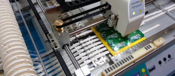
There are many, many ways to get a PCB design onto a board for etching. Even with practice however, the quality of the result varies with the process and equipment used. With QFN parts becoming the norm, the days of etch-resist transfers and a permanent marker are all but gone. Luckily, new and improved methods of Gerber transfer have be devised in recent years thanks to hackers across the world.
One such hacker, [Henner] is working on a project called LDGraphy in an attempt to bring high-resolution etching to the masses. LDGraphy is a laser lithography device that makes use of a laser and a Beaglebone green to etch the layout onto the board. The best part is that the entire BOM is claimed to cost under a $100 which makes it affordable to people on a budget.
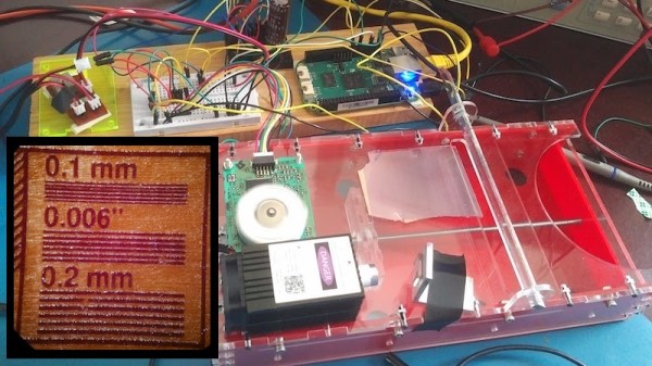
The system is designed around a 500 mW laser and a polygon mirror scanner meant for a laser printer. The board with photoresist is linearly actuated in the X-axis using a stepper motor and the laser beam which is bounced off the rotating hexagonal mirror is responsible for the Y-axis. The time critical code for the Programmable Realtime Unit (PRU) of the AM335X processor is written in assembly for the fast laser switching. The enclosure is, naturally, a laser cut acrylic case and is made at [Henner]’s local hackerspace.
[Henner] has been hard at work calibrating his design and compensating for the inaccuracies of the components used. In the demo video below he presents a working version with a resolution of 6 mils which is wonderful considering the cost of the machine. He also shares his code on GitHub if you want to help out and you can track his updates on Google+. Continue reading “Laser PCBs With LDGraphy”