Instead of mucking about fabbing PCBs with the toner transfer method, or making masks for photosensitive boards, the holy grail of at-home circuit board manufacturing is a direct inkjet-to-etch method. [Don] isn’t quite there yet, but his method of producing circuit boards at home is one of the easiest we’ve ever seen.
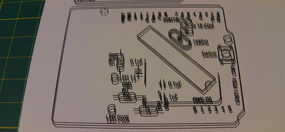
[Don]’s boards begin by taking the output from Eagle and printing them with an Epson Artisan 50 inkjet printer. By sticking a piece of cardstock in the printer before the copper board, he’s able to precisely align the traces and pads onto the copper board.
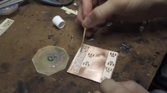
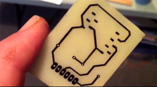
When the board comes out of the printer, it’s only covered in ink. While some specialty inks are enough of an etch resist, [Don] comes up with a clever way to make sure acid doesn’t eat away copper in the needed places – he simply dusts on toner from a copier or laser printer, blows off the excess, and bakes the entire board in a toaster oven.
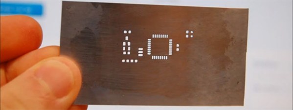
The result, seen above, are perfect traces on a circuit board without the need for ironing sheets of photo paper onto copper boards.
As far as the, “why didn’t someone think of this sooner” ideas go, this one is at the top. [Don] says the method should work on sheets of aluminum for printing solder paste masks. Impressive work, and now the only thing left to do is getting two-layer boards down pat. For more direct to copper printing check out the hacks we’ve covered in years past.