Dead-Bug Logic Probe In A Magic Marker

Logic probes are simple but handy tools that can be had for a couple of bucks. They may not be the sexiest pieces of test gear, nor the most versatile, but they have their place, and building your own logic probe is a great way to understand the tool’s strength and weaknesses.

[Jxnblk]’s take on the logic probe is based on a circuit by [Tony van Roon]. The design hearkens back to a simpler time and is based on components that would have been easy to pick up at any Radio Shack once upon a time. The logic section is centered on the venerable 7400 quad 2-input NAND gate in the classic 14-pin DIP format. The gates light separate LEDs for high and low logic levels, and a 555 timer chip in a one-shot configuration acts as a pulse stretcher to catch transients. The DIP packages lend themselves to quick and dirty “dead bug” construction, and the whole thing fits nicely into a discarded marking pen.

dead-bug-logic-probe-in-marker-body

It’s a simple build and a nice form factor for a useful tool, but for an even slimmer package like an old syringe you’ll probably have to go with SMD components. And when you graduate from the simple logic probe, you might want to check out the capabilities of this smart probe.

Hackaday Prize Entry: You Can Do Anything With A Bunch Of NANDs

Every few years, someone on the Internet builds a truly homebrew CPU. Not one built with a 6502, Z80, or a CPU from the 80s, either: one built completely out of 74-series logic chips or discrete transistor. We’re lucky enough to have [Alexander] document his build on Hackaday.io, and even luckier to have him enter it into this year’s Hackaday Prize. It’s an 8-bit computer built completely out of NAND gates.

Computers are just logic, and with enough NAND gates, you can do anything. That’s exactly what [Alex] is doing with this computer. It’s built entirely out of 74F00 chips – a ‘fast’ version of the ubiquitous quad 2-input NAND chip. The architecture of this computer borrows from the best CPUs of the 70s and 80s. The ALU is only four bits, like the Z80, but also uses the 6502 technique where the borrow is an inverted carry. It’s a small instruction set, a 2-stage pipeline, and should be able to compute one million instructions per second.

Designing a CPU is one thing, and thanks to Logisim, this is already done. Constructing a CPU is another matter entirely. For this, [Alex] is going for a module and backplane approach, where the ALU is constructed of a few identical modules tied together into a gigantic motherboard. [Alex] isn’t stopping at a CPU, either: he has a 16-byte ROM that’s programmed by plugging diodes into holes.

It’s an amazingly ambitious project, and for entering this project into the 2016 Hackaday Prize, [Alex] already netted himself $1000 and a trip to the final round of competition.

The HackadayPrize2016 is Sponsored by:

Hackaday Prize Entry: From Q To NAND

The apocalypse is coming, and the last time I checked, not many people have a semiconductor fab in their garage. We’ll need computers after the end of the world, and [matseng]’s project for the Hackaday Prize is just that – a framework to build computers out of discrete components.

The apocalyptic spin on this project is slightly exaggerated, but there is a lot someone can learn by building digital devices out of transistors, resistors, and diodes. The building blocks of [matseng]’s computer are as simple as they come: he’s using three resistors, four diodes, and one NPN transistor to build a single NAND gate. These NAND gates can then be assembled into any form of digital logic. You’re never going to get a better visual example of functional completeness.

A project like this must be approached from both the top down and bottom up. To go from a high level to ones and zeros, [matseng] built an assembler and an emulator. Some ideas of what the instruction set will be are laid out in this project log, and for now [matseng] is going for a Harvard architecture with eight registers. It’s a lot of work for a computer that will be limited by how much memory [matseng] can be wired up, but as far as ambition goes, there aren’t many projects in the Hackaday Prize that can match this tiny, huge computer.

The 2015 Hackaday Prize is sponsored by:

The Flaming Yinlips

furan-yinlips

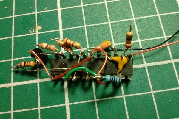
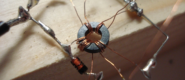
No, that’s not a Playstation Vita up there, it’s a “Yinlips YDPG18A” portable game system. [Ian] found that his Yinlips was lacking in the flash memory department, so he fired up his soldering iron. The Yinlips is based on an Allwinner Sunxi series processor, and uses a standard TSOP48 footprint flash. There is some standardization in flash pin out and packages, so [Ian] picked up the largest pin compatible chips he could find – a pair of 256 gigabit (32 gigabyte) chips from Micron. Desoldering the existing flash proved to be a bit of an adventure as the flash was glued down. [Ian] also didn’t have his hot air gun handy, making things even more interesting. Careful work with a razor blade broke the glue bond.

It turns out that the soldering was the easy part. All flash chips have geometry, die count, page size, block count, sector size, etc. The geometry is similar to the geometry in a hard drive. In fact, just like in modern hard drives, a system will read some basic information before accessing the full storage array. In the case of NAND flash, the processor can access the first page of memory, and query the flash for its part number. Once the part number is known, the geometry can be determined via a lookup table. [Ian] checked the NAND table on github, so he knew going in that his flash chips were not supported. Due to the complexities of booting Allwinner processors into Linux or Android, the table and the NAND driver that uses it exist in several places. The bootloader’s axf file, U-Boot, and several flash application binaries sent from the PC based LiveSuit flash app all required modification. Most of these files were packed into a single flash image. [Ian] used imgrepacker to unpack the image, then opened the hex files. The fact that he knew what the original flash parameter tables looked like was key. He searched for an existing Micron flash table entry, and replaced the parameters with those of his new chips.

With all the files modified, [Ian] re-packed his flash image and sent it over. The Yinlips rewarded his hard work by continually resetting in a bootloop. [Ian] wasn’t going to give up though. He wired into the boot console, and discovered that a CRC check failure on one of his modified files was causing the reset. He then disassembled binary issuing the reset. Changing the return value of the CRC to always pass fixed the issue. [Ian’s] now has a collagen infused Yinlips with 58GB of internal storage. Pretty good for a device that only started with 2GB.

Making Logic With Inductors

NOR

We’ve seen NAND and NOR logic gates – the building blocks of everything digital – made out of everything from marbles to Minecraft redstone. [kos] has outdone himself this time with a logic circuit we’ve never seen before. It’s based on magnets and induction, making a NOR gate out of nothing but a ferrite core, some wire, and a diode.

The theory of operations for this magnetic NOR gate goes as follows: If two of the input windings around the core have current passing in different directions, the fields cancel out. This could either be done by positive or negative voltages, or by simply changing the phase of the winding. To keep things simple, [kos] chose the latter. The truth table for a simple two-input, one-output gate gets pretty complicated (or exceedingly cool if you’d like to build a trinary computer), so to get absolute values of 1 and 0, a separate ‘clock’ winding was also added to the core.

One thing to note about [kos]’ gate is its innovation on techniques described in the relevant literature. Previously, these kinds of magnetic gates were built with square ferrites, while this version can work with any magnetic core.

While this isn’t a very practical approach towards building anything more complex than a memory cell, it is an exercise of what could have been in an alternate universe where tube technology and the transistor just didn’t happen.

NANDputer Is Mostly Wiring

We would wager that by weight this project is mostly wiring. We might go as far as betting that the wire outweighs the rest of the components 2 to 1. We’ll keep our fingers crossed that there’s never a loose connection, but for now it seems that [Kevin Horton’s] NAND-based computer project is up and running. Very nearly ever part of the build is based on NAND gates, which is why the point-to-point wiring is so crazy. There is one peripheral board which uses some non-NAND components, but he eventually plans on replacing that to make the system…. pure?

Now get ready for the crazy part. This is just one half of the program counter! There’s another board that looks just like it. The two join at least a half-dozen other boards of similar size and complexity to make a functioning computer. Crazy! The post shares a ton of details, but you can also just skip down after the break to see a video of it running a program.

If you’re wondering how a NAND-based computer works you should make your way through this online course.

Continue reading “NANDputer Is Mostly Wiring”

Wireless Pinball Controller For Tablet Gaming

wireless-pinball-controller

This wooden box is a wireless pinball controller and tablet stand. The idea is to set it on a workbench to give you some of the thrill of standing and playing the real thing. [Jeff] has been rather addicted to playing a pinball app on Android lately, and started the journey because he needed a way to give his thumbs some relief.

An Arduino monitors buttons on either side of this wooden controller. [Jeff] is new to working with hardware (he’s a Linux Kernel developer by trade) and was immediately struck with button debouncing issues. Rather than handle this in software (we’ve got a super-messy thread on that issue with our favorite at the bottom) he chose a hardware solution by building an SR latch out of two NAND gates.

With the inputs sorted out he added a BlueSMiRF board to the project which allowed him to connect a Nexus 7 tablet via Bluetooth. At this point he ran into some problems getting the device to respond to his control as if it were an external keyboard. His stop-gap solution was to switch to a Galaxy Tab 10.1 which wasn’t throwing cryptic errors. Hopefully he’ll fix this in the next iteration which will also include adding a plunger to launch the pinball, a part which just arrived in the mail as he was writing up this success.

We’ve embedded his quick demo video after the break.

Continue reading “Wireless Pinball Controller For Tablet Gaming”