Since Autodesk acquired Eagle a few years ago, they’ve been throwing out all the stops. There is now a button in Eagle that flips your board from the front to the back — a feature that should have been there twenty years ago. There’s parametric part generation, push and shove routing, integration with Fusion 360, and a host of other features that makes Eagle one of the best PCB layout tools available.
Today, Autodesk is introducing something revolutionary. The latest version of Eagle (version 8.7.1) comes with a manual serpentine routing mode, giving anyone the same tools as the geniuses at Nokia twenty years ago.
An exclusive first look at Eagle’s new serpentine routing mode
The new serpentine routing mode is invoked via the SNAKE command. This brings up serpentine routing interface, where you can add nets and place your serpentine router. Click anywhere on the screen, and you can route around pads and traces to collect all the vias, hopefully netting a high score.
There are some tricks to this new mode. Control and Shift change the speed of serpentine routing, and the current zoom level changes the initial speed. As you route between vias, the serpentine router grows longer, making routing significantly more difficult, but if you’re up to the task you’ll eventually get a ‘You’re Winner’ screen.
This is just the innovation we’ve been looking for from Autodesk since their acquisition of Eagle. It’s not push and shove routing, and it’s not parametric part generation. Serpentine routing is the next big thing in EDA tools, and already this routing mode is on the upcoming feature list for KiCad. The KiCad version of serpentine routing will be pronounced, ‘sneak’.
The semiconductor devices were put to the test under different atmospheres in this chamber.
One of the humbling things about writing for Hackaday comes when we encounter our readership and learn the breadth of our community and the huge variety of skills and professions you represent. Among your number are a significant representation among scientists, and as a result we often receive fascinating previews of and insights into their work. Sometimes they deserve a little bit more attention than one of our normal short daily pieces, and such a moment has come our way this week.
We’ve been fortunate enough to have an early look at a paper which makes detailed observations of a hitherto barely characterised property of semiconductor junctions that might have some interest for Hackaday readers in their work. In their paper, [Mellie], [Bacon] et al at Fulchester University in northeast England take a look at incandescent luminescence, a fleeting and curious effect exhibited by all semiconductor junctions in which they emit short-duration high-intensity infra-red and visible light with an extremely fast rise time when presented with high levels of current. This is a property which has been rarely exploited in commercial devices due to the large current densities required to reproduce it.
Incandescent Luminescence Explained
If you’ve never heard of incandescent luminescence before then you’re in good company, for neither had we until it was explained to us. It appears that there are a set of higher energy state conductivity bands in a semiconductor junction that can only be reached once the current passing through it breaches a threshold governed by the available quantum plasma dipole moment of the semiconductor material in question. At this point the junction assumes a plasma condition resulting in the abrupt emission of infra-red and visible radiation, the incandescent luminescence phase has been triggered.
A near-infra-red spectrum of incandescent luminescence in a silicon semiconductor junction.
Though it has been known to science since first being observed in the early 20th century by the earliest experimenters in the field of semiconductor junctions, the transitory nature of the phenomenon has traditionally been a barrier to its proper examination. The British team took a selection of commercial semiconductor devices very similar to the types that might be used by Hackaday readers, placed them in a chamber, and used an array of photoelectric sensors coupled with ionising detectors using americium-241 alpha radiation sources to measure their emissions.
The resulting data was then harvested for processing through a stack of custom high-speed ADC cards. Current densities from as low as a few milliamps to hundreds of amps were tested across forward-biased PN diode junctions using a computer-controlled DC power supply, resulting in a variety of spectra and showing the resulting thermionic photon emission at higher currents to have a preponderance in the infra-red region.
Incandescent luminescence in action, through an infra-red pyrometer.
A series of experiments were conducted to investigate a related effect first described by those early scientists in the field: that the atmosphere in which the semiconductor junction sits has a significant effect on the way it exhibits incandescent luminescence. Bathing it in gaseous CO₂ or nitrogen was found to reduce the phenomenon by as much as 95%, while immersing it in liquid nitrogen resulted in it becoming completely unobservable. Oxygen-rich atmospheres by comparison served to enhance the luminescence observed, to the point that in one of pure oxygen it reached an efficiency level of 100%.
The high conversion efficiencies and rapid onset of incandescent luminescence once it has been triggered compares favourably to those of existing devices such as LEDs or wire-wound resistors used where either infra-red or visible light is required. The researchers expect the effect to be exploited in such product families as photographic flash generators, electronic igniters, and other short-duration high-intensity applications. Given their obvious advantages, we’d expect their effects on those particular markets to be nothing short of incendiary.
Thanks Ellie D. Martin-Eberhardt for some invaluable inspiration and technical help with covering this story.
Get ready for another step towards our dystopian future as scientists have invented a way to track and monitor what we eat. This 2mm x 2mm wireless sensor can be mounted on to teeth and can track everything that goes into your mouth. Currently it can monitor salt, glucose, and alcohol intake. The sensor then communicates wirelessly to a mobile device that tracks the data. Future revisions are predicted to monitor a wide range of nutrients and chemicals that can get ingested.
It uses an interesting method to both sense the target chemicals and communicate its data. It consists of a sandwich of three layers with the central layer being a biosensor that reacts to certain chemicals. The complete sandwich forms a tiny RFID antenna and when RF signals are transmitted to the device, some of the signal gets absorbed by the antenna and the rest reflected back.
The mechanism is similar to how chromatography works for chemical analysis where certain chemicals absorb light wavelengths of specific frequencies. Passing a calibrated light source through a gas column and observing the parts of the spectrum that get absorbed allows researchers to identify certain chemicals inside the column.
This technology is based on previous research with”tooth tatoos” that could be used by dentists to monitor your oral health. Now this tiny wireless sensor has evolved to monitoring the dietary intake of people for health purposes but we’re pretty sure Facebook is eyeing it for more nefarious purposes too.
Recently, one of [Eric]’s clients asked him to design a bottle. Simple enough for a product designer, except that the client needed it to thread into a specific type of cap. And no, they don’t know the specs.
But that’s no problem, thought [Eric] as he turned on the exhaust fan and reached for the secret ingredient that would make casting the negative image of the threads a breeze. He mixed up the foul-smelling body filler with the requisite hardener and some lovely cyan toner powder and packed it into the cap with a tongue depressor. Then he capped off the cast by adding a small PVC collar to lengthen the cast so he has something to grab on to when it’s time to take it out.
Bondo does seem like a good choice for casting threads. You need something workable enough to twist out of there without breaking, but rigid enough that the small detail of the threads isn’t lost. For the release agent, [Eric] used Johnson’s Paste Wax. He notes from experience that it works particularly well with Bondo, and even seems to help it cure.
Once the Bondo hardened, [Eric] made sure it screwed in and out of the cap and then moved on to CAD modeling and 3D printing bottle prototypes until he was satisfied. We’ve got the video screwed in after the break to cap things off.
One of the things that every student of digital electronics learns, is that every single logic function can be made from a combination of NAND gates. But nobody is foolhardy enough to give it a try, after all that would require a truly huge number of gates!
Someone evidently forgot to tell [Notbookies], for he has made a complete 8-bit ALU using only 4011B quad NAND gates on a set of breadboards, and in doing so has created a minor masterpiece with his wiring. It’s inspired by a series of videos from [Ben Eater] describing the construction of a computer with the so-called SAP (Simple As Possible) architecture. The 48 4011B DIP packages sit upon 8 standard breadboards, with an extra one for a set of DIP switches and LEDs, and a set of power busbar breadboards up their sides. He leaves us with the advice borne of bitter experience: “Unless your goal is building a NAND-only computer, pick the best IC for the job“.
We have covered countless processors and processor components manufactured from discrete logic chips over the years, though this makes them no less impressive a feat. The NedoNAND has been a recent example, a modular PCB-based design. TTL and CMOS logic chips made their debut over 50 years ago so you might expect there to be nothing new from that direction, however we expect this to be well of projects that will keep flowing for may years more.
[Ivan] has been keeping his 3D printers busy with parts he’s experimenting with to build a tracked motion setup for a tank-like vehicle. His design uses several interlocking parts, so if you want to duplicate it, we hope your printer calibration is up to snuff. He’s still printing more parts and promises to release the files once the design proves out.
However, you can see he’s off to a good start. Small pieces fit together and accept a piece of filament as a sort of hinge. Some pins keep the filament from working out. Pads fit into the main parts and hold down with zip ties. The whole flexible tread locks into sprockets and a groove on a drive wheel.
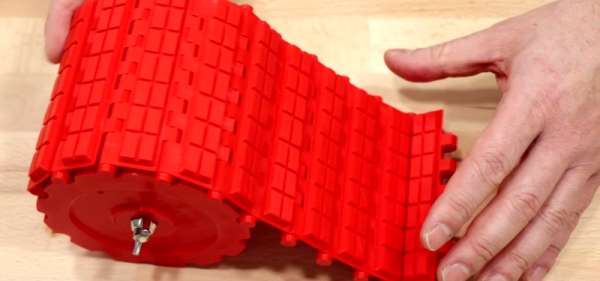
LoRa and LPWANs (Low Power Wide Area Networks) are all the range (tee-hee!) in wireless these days. LoRa is a sub 1-GHz wireless technology using sophisticated signal processing and modulation techniques to achieve long-range communications.
With that simplified introduction, [Omkar Joglekar] designed his own LoRa node used for outdoor sensor monitoring based on the HopeRF RFM95 LoRa module. It’s housed in an IP68 weatherproof enclosure and features an antenna that was built from scratch using repurposed copper rods. He wrote up the complete build, materials, and description which makes it possible for others to try their hand at putting together their own complete LoRa node for outdoor monitoring applications.