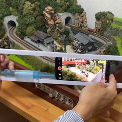
We love the idea [Btoretsukuru] shared that uses a simple setup called the Syringe Slider to take smoothly-tracked video footage of small scenes like model trains in action. The post is in Japanese, but the video is very much “show, don’t tell” and it’s perfectly clear how it all works. The results look fantastic!
Suited to filming small subjects.
The device consists of a frame that forms a sort of enclosed track in which one’s mobile phone can slide horizontally. The phone butts up against the plunger of an ordinary syringe built into the frame. As the phone is pushed along, it depresses the plunger which puts up enough resistance to turn the phone’s slide into a slow, even, and smooth glide. Want to fine-tune the resistance and therefore the performance? Simply attach different diameter tips to the syringe.
The results speak for themselves, and it’s a fantastically clever bit of work. There are plenty of DIY slider designs (some of which get amazingly complex) but they are rarely small things that can be easily gotten up close and personal with small subjects like mini train terrain.
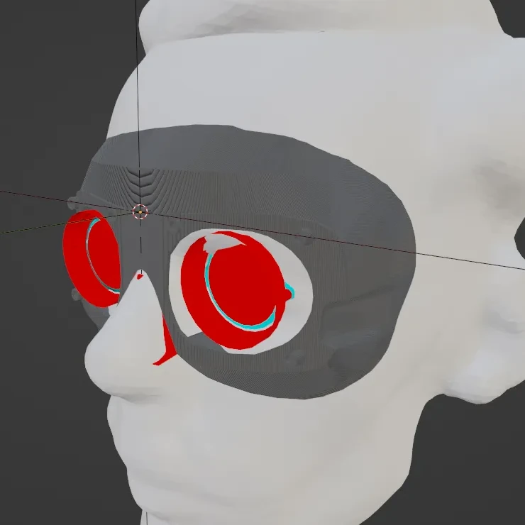
The Bigscreen Beyond is a small and lightweight VR headset that in part achieves its small size and weight by requiring custom fitting based on a facial scan. [Val’s Virtuals] managed to improve fitment even more by redesigning a facial interface and using a 3D scan of one’s own head to fine-tune the result even further. The new designs distribute weight more evenly while also providing an optional flip-up connection.
It may be true that only a minority of people own a Bigscreen Beyond headset, and even fewer of them are willing to DIY their own custom facial interface. But [Val]’s workflow and directions for using Blender to combine a 3D scan of one’s face with his redesigned parts to create a custom-fitted, foam-lined facial interface is good reading, and worth keeping in mind for anyone who designs wearables that could benefit from custom fitting. It’s all spelled out in the project’s documentation — look for the .txt file among the 3D models.
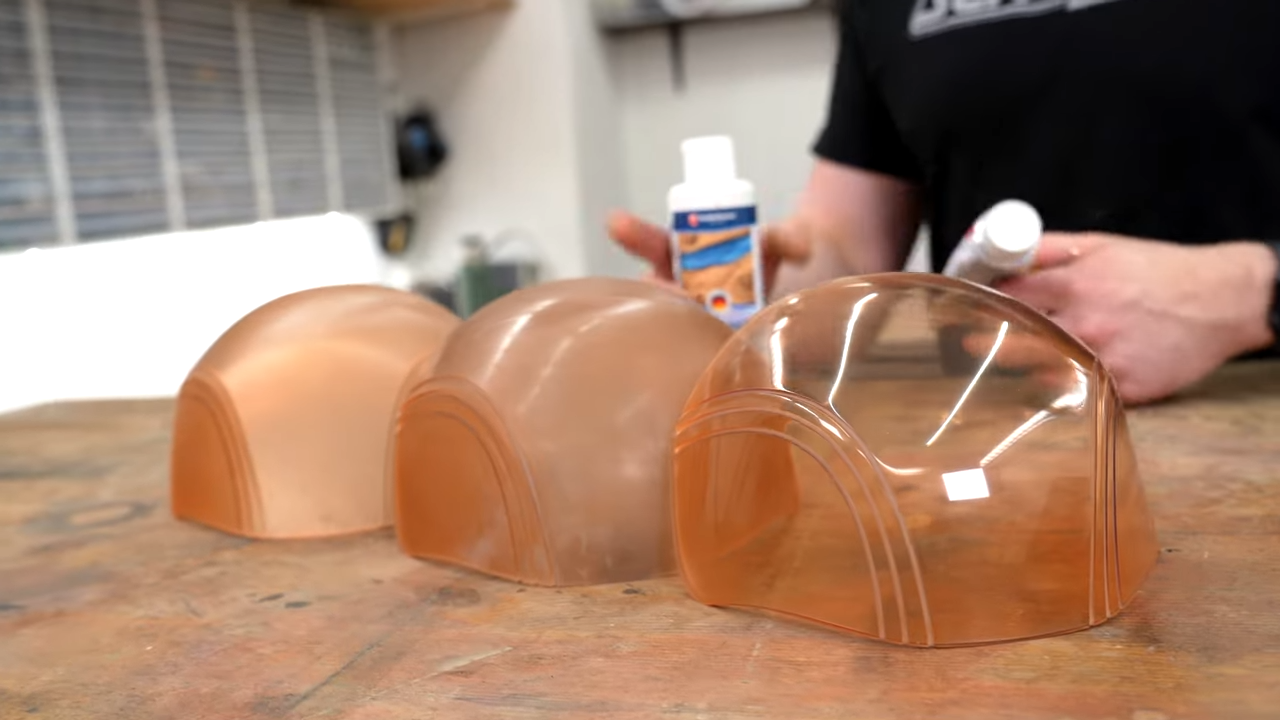
[Zibartas] recently created wearable helmets from the game Starfield that look fantastic, and we’re happy to see that he created a video showcasing the whole process of design, manufacture, and assembly. The video really highlights just how much good old-fashioned manual work like sanding goes into getting good results, even in an era where fancy modern equipment like 3D printing is available to just about anyone.
The secret to perfectly-tinted and glassy-smooth clear visors? Lots and lots of sanding and polishing.
The visor, for example, is one such example. The usual approach to making a custom helmet visor (like for Daft Punk helmet builds) is some kind of thermoforming. However, the Starfield helmet visors were poor candidates due to their shape and color. [Zibartas]’s solution was to 3D print the whole visor in custom-tinted resin, followed by lots and lots of sanding and polishing to obtain a clear and glassy-smooth end product.
A lot of patient sanding ended up being necessary for other reasons as well. Each helmet has a staggering number of individual parts, most of which are 3D printed with resin, and these parts didn’t always fit together perfectly well.
[Zibartas] also ended up spending a lot of time troubleshooting an issue that many of us might have had an easier time recognizing and addressing. The helmet cleverly integrates a faux-neon style RGB LED strip for internal lighting, but the LED strip would glitch out when the ventilation fan was turned on. The solution after a lot of troubleshooting ended up being simple decoupling capacitors, helping to isolate the microcontrollers built into the LED strip from the inductive load of the motors.
What [Zibartas] may have lacked in the finer points of electronics, he certainly makes up for in practical experience when it comes to wearable pieces like these. The helmets look solid but are in fact full of open spaces and hollow, porous surfaces. This makes them more challenging to design and assemble, but it pays off in spades when worn. The helmets not only look great, but allow a huge amount of airflow. This along with the fans makes them comfortable to wear as well as prevents the face shield from misting up from the wearer’s breathing. It’s a real work of art, so check out the build video, embedded just below.
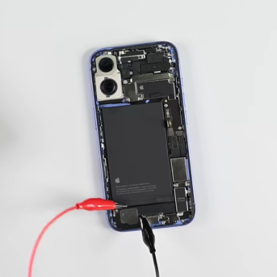
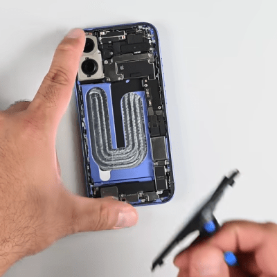
There’s a wild new feature making repair jobs easier (not to mention less messy) and iFixit covers it in their roundup of the iPhone 16’s repairability: electrically-released adhesive.
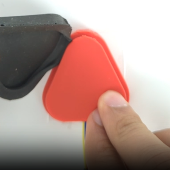
Here’s how it works. The adhesive looks like a curved strip with what appears to be a thin film of aluminum embedded into it. It’s applied much like any other adhesive strip: peel away the film, and press it between whatever two things it needs to stick. But to release it, that’s where the magic happens. One applies a voltage (a 9 V battery will do the job) between the aluminum frame of the phone and a special tab on the battery. In about a minute the battery will come away with no force, and residue-free.
9V does the job in about a minute, but up to 30 V can be used.
The battery comes away cleanly and without leaving residue.
There is one catch: make sure the polarity is correct! The adhesive releases because applying voltage oxidizes aluminum a small amount, causing Al3+ to migrate into the adhesive and debond it. One wants the adhesive debonded from the phone’s frame (negative) and left on the battery. Flipping the polarity will debond the adhesive the wrong way around, leaving the adhesive on the phone instead.
Some months ago we shared that Apple was likely going to go in this direction but it’s great to see some hands-on and see it in action. This adhesive does seem to match electrical debonding offered by a company called Tesa, and there’s a research paper describing it.
A video embedded below goes through the iPhone 16’s repairability innovations, but if you’d like to skip straight to the nifty new battery adhesive, that starts at the 2:36 mark.
There are a number of ways to give a robotic actuator a sense of touch, but the AnySkin project aims to make it an overall more reliable and practical process. The idea is twofold: create modular grippy “skins” that can be slipped onto actuators, and separate the sensing electronics from the skins themselves. The whole system ends up being quite small, as shown here.
Cast skins can be installed onto bases as easily as slipping a phone case onto a phone.
The skins are cast in whatever shape is called for by using silicone (using an off-the-shelf formulation from Smooth-on) mixed with iron particles. This skin is then slipped onto a base that contains the electronics, but first it is magnetized with a pulse magnetizer. It’s the magnetic field that is at the heart of how the system works.
The base contains five MLX90393 triple-axis magnetometers, each capable of sensing tiny changes in magnetic fields. When the magnetized skin over the base is deformed — no matter how slightly — its magnetic field changes in distinct ways that paint an impressively detailed picture of exactly what is happening at the sensor. As a bonus, slippage of the skin against the sensor (a kind of shearing) can also be distinctly detected with a high degree of accuracy.
The result is a durable and swappable robotic skin that can be cast in whatever shape is needed, itself contains no electronics, and can even be changed without needing to re-calibrate everything. Cameras can also sense touch with a high degree of accuracy, but camera-based sensors put constraints on the size and shape of the end result.
AnySkin builds on another project called ReSkin and in fact uses the same sensor PCB (design files and bill of materials available here) but provides a streamlined process to create swappable skins, and has pre-made models for a variety of different robot arms.
When are jumper wires on a breadboard entirely optional? When it’s the latest version of [Kevin Santo Cappuccio]’s Jumperless, which uses a bunch of analog crosspoint switches (typically used for handling things like video signals) to create connections instead of physical wires. There’s even an RGB LED under each hole capable of real-time visualization of signals between components.
If this looks a bit familiar, that’s because an earlier version took second place in the 2023 Hackaday Prize. But things have evolved considerably since then. There are multiple programmable power rails, ADC channels, a rotary encoder, and much more. The PCB design itself is fantastic, including the probe which acts like a multi-function tool for interacting with the whole thing. The newest version will make its debut on Crowd Supply in just a few days.
It’s open source and made to be hackable, so give the GitHub repository a look if you want a closer peek. You can watch it in action in a brief video posted to social media, embedded below.
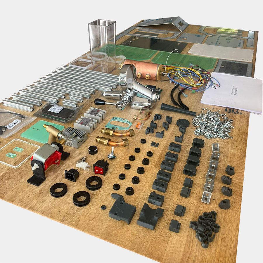
Want to build your own espresso machine, complete with open-source software to drive it? The diyPresso might be right up your alley.
diyPresso parts, laid out and ready for assembly.
It might not be the cheapest road to obtaining an espresso machine, but it’s probably the most economical way to turn high-quality components (including a custom-designed boiler) and sensors into a machine of a proven design.
Coffee and the machines that turn it into a delicious beverage are fertile ground for the type of folk who like to measure, modify, and optimize. We’ve seen DIY roasters, grinders, and even a manual lever espresso machine. There are also many efforts at modifying existing machines with improved software-driven controls but this is the first time we’ve seen such a focused effort at bringing the DIY angle to a ground-up espresso machine specifically offered as a kit.
Curious to know more? Browse the assembly manual or take a peek at the software’s GitHub repository. You might feel some ideas start to flow for your next coffee hack.